Description
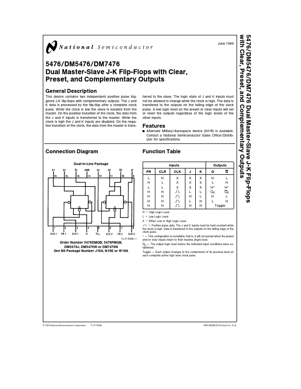
This device contains two independent positive pulse triggered J-K flip-flops with complementary outputs The J and K data is processed by the flip-flop after a complete clock pulse While the clock is low the slave is isolated from the master On the positive transition of the clock the data from the J and K inputs is transferred to the master While the clock is high the J and K inputs are disabled On the negative transition of the clock the data from the master is trans- ferred to the slave The logic state of J and K inputs must not be allowed to change while the clock is high The data is transfered to the outputs on the falling edge of the clock pulse A low logic level on the preset or clear inputs will set or reset the outputs regardless of the logic levels of the other inputs.