Description
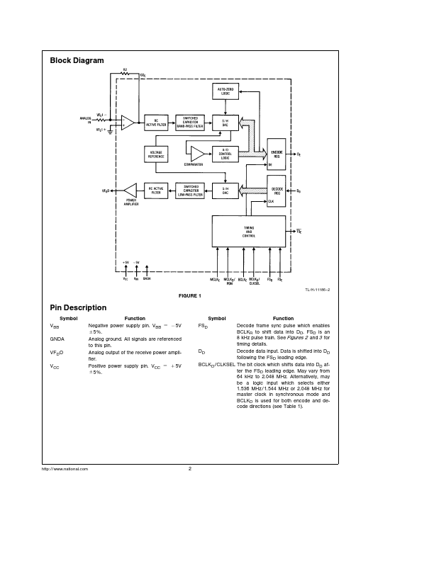
The TP5510 consists of a m-law monolithic AFE device utilizing the A D and D A conversion architecture shown in Figure 1 and a serial data interface The device is fabricated using National’s advanced double-poly CMOS process (microCMOS) The A D portion of the device consists of an input gain adjust amplifier an active RC pre-filter which eliminates very high frequency noise and a switched-capacitor band-pass filter that rejects signals below 200 Hz and above 3400 Hz Also included are auto-zero c
Features
- Y
Y Y Y Y Y Y Y Y Y Y Y Y
Complete A D and D A with filter system including Serial Data Interface Encode high-pass and low-pass filter Decode low-pass filter with sin x x correction Active RC noise filters m-law compatible A D and D A Internal precision voltage reference Internal auto-zero circuitry m-law TP5510 g 5V operation Low operating power typically 60 mW Power-down standby mode typically 3 mW Automatic power-down TTL or CMOS compatible digital interfaces Maximizes PC card circuit densi.
 TP5510_NationalSemiconductor.pdf