FDB035N10A Overview
Key Specifications
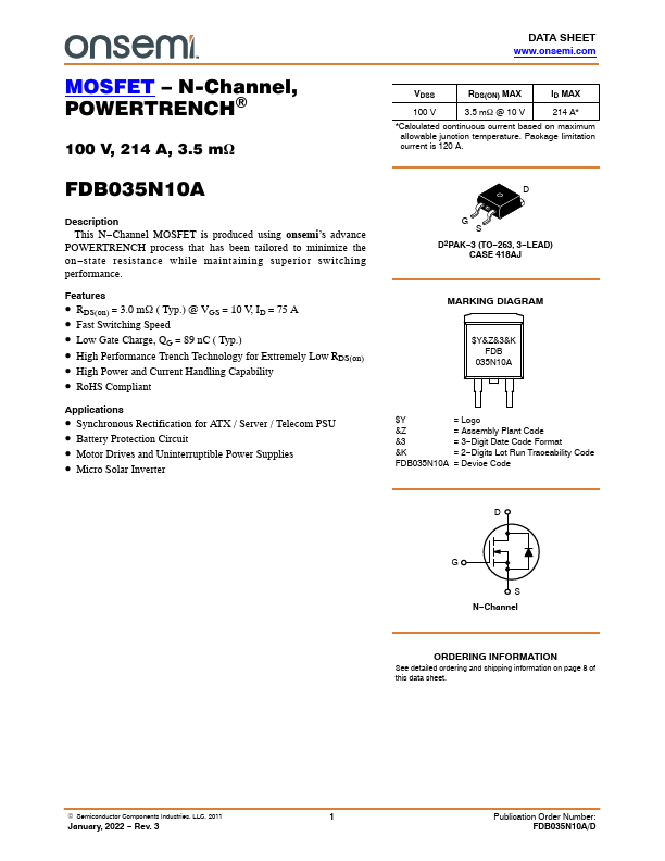
Package: D2PAK
Mount Type: Surface Mount
Pins: 3
Height: 5.08 mm
Description
This N-Channel MOSFET is produced using onsemi’s advance POWERTRENCH process that has been tailored to minimize the on-state resistance while maintaining superior switching performance.
Key Features
- RDS(on) = 3.0 mW ( Typ.) @ VGS = 10 V, ID = 75 A
- Fast Switching Speed
- Low Gate Charge, QG = 89 nC ( Typ.)
- High Performance Trench Technology for Extremely Low RDS(on)
- High Power and Current Handling Capability