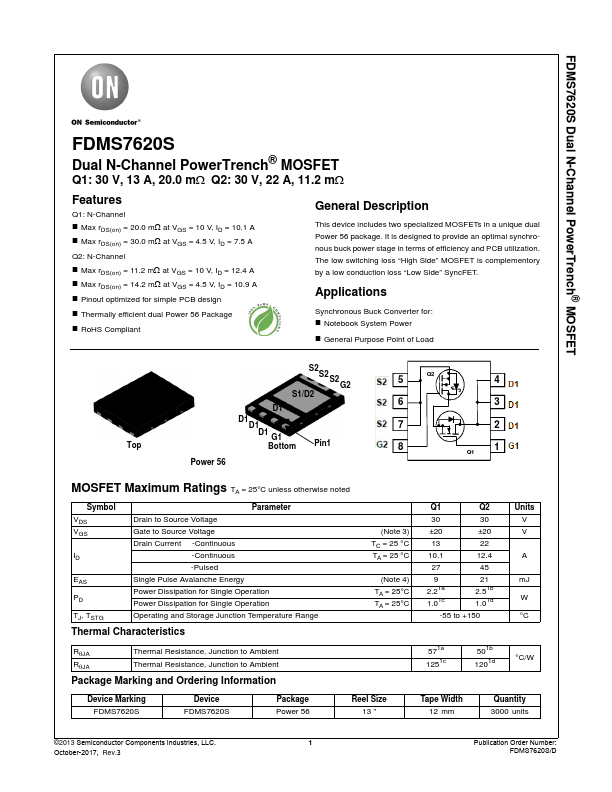
Datasheet4U Logo Datasheet4U.com

FDMS7620S - Dual N-Channel MOSFET

Description

This device includes two specialized MOSFETs in a unique dual Power 56 package.

It is designed to provide an optimal synchronous buck power stage in terms of efficiency and PCB utilization.

The low switching loss “High Side” MOSFET is complementory by a low conduction loss “Low Side” SyncFET.

Features

  • Q1: N-Channel.
  • Max rDS(on) = 20.0 mΩ at VGS = 10 V, ID = 10.1 A.
  • Max rDS(on) = 30.0 mΩ at VGS = 4.5 V, ID = 7.5 A Q2: N-Channel.
  • Max rDS(on) = 11.2 mΩ at VGS = 10 V, ID = 12.4 A.
  • Max rDS(on) = 14.2 mΩ at VGS = 4.5 V, ID = 10.9 A.
  • Pinout optimized for simple PCB design.
  • Thermally efficient dual Power 56 Package.
  • RoHS Compliant General.

📥 Download Datasheet

Datasheet preview – FDMS7620S

Datasheet Details

Part number FDMS7620S
Manufacturer ON Semiconductor
File Size 432.95 KB
Description Dual N-Channel MOSFET
Datasheet download datasheet FDMS7620S Datasheet
Additional preview pages of the FDMS7620S datasheet.
Other Datasheets by ON Semiconductor

Full PDF Text Transcription

Click to expand full text
FDMS7620S Dual N-Channel PowerTrench® MOSFET FDMS7620S Dual N-Channel PowerTrench® MOSFET Q1: 30 V, 13 A, 20.0 mΩ Q2: 30 V, 22 A, 11.2 mΩ Features Q1: N-Channel „ Max rDS(on) = 20.0 mΩ at VGS = 10 V, ID = 10.1 A „ Max rDS(on) = 30.0 mΩ at VGS = 4.5 V, ID = 7.5 A Q2: N-Channel „ Max rDS(on) = 11.2 mΩ at VGS = 10 V, ID = 12.4 A „ Max rDS(on) = 14.2 mΩ at VGS = 4.5 V, ID = 10.9 A „ Pinout optimized for simple PCB design „ Thermally efficient dual Power 56 Package „ RoHS Compliant General Description This device includes two specialized MOSFETs in a unique dual Power 56 package. It is designed to provide an optimal synchronous buck power stage in terms of efficiency and PCB utilization. The low switching loss “High Side” MOSFET is complementory by a low conduction loss “Low Side” SyncFET.
Published: |