Datasheet Details
| Part number | MC100LVEL05 |
|---|---|
| Manufacturer | onsemi |
| File Size | 140.07 KB |
| Description | 2-Input Differential AND/NAND |
| Datasheet | MC100LVEL05_ONSemiconductor.pdf |
|
|
Overview: MC100LVEL05 3.3 V ECL 2‐Input Differential AND/NAND.
| Part number | MC100LVEL05 |
|---|---|
| Manufacturer | onsemi |
| File Size | 140.07 KB |
| Description | 2-Input Differential AND/NAND |
| Datasheet | MC100LVEL05_ONSemiconductor.pdf |
|
|
|
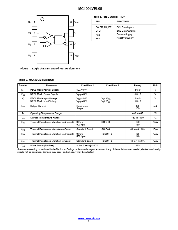
The MC100LVEL05 is a 2-input differential AND/NAND gate.
The device is functionally equivalent to the MC100EL05 device and operates from a 3.3 V supply voltage.
With propagation delays and output transition times equivalent to the EL05, the LVEL05 is ideally suited for those applications which require the ultimate in AC performance at low voltage power supplies.
| Brand Logo | Part Number | Description | Manufacturer |
|---|---|---|---|
| MC100LVEL05 | 2-Input Differential AND/NAND | Motorola |
| Part Number | Description |
|---|---|
| MC100LVEL01 | 4-Input OR/NOR |
| MC100LVEL11 | Low Voltage 1:2 Differential Fanout Buffer |
| MC100LVEL12 | Low Impedance Driver |
| MC100LVEL13 | Dual 1:3 Fanout Buffer |
| MC100LVEL14 | 1:5 Clock Distribution Chip |
| MC100LVEL16 | Differential Receiver |
| MC100LVEL17 | Quad Differential Receiver |
| MC100LVEL29 | Dual Differential Data and Clock D Flip-Flop |
| MC100LVEL30 | Triple D Flip-Flop |
| MC100LVEL31 | 3.3V ECL D Flip?Flop |