Datasheet Details
| Part number | MC100LVEL14 |
|---|---|
| Manufacturer | ON Semiconductor |
| File Size | 138.13 KB |
| Description | 1:5 Clock Distribution Chip |
| Datasheet |
 MC100LVEL14 Datasheet MC100LVEL14 Datasheet
|
|
|
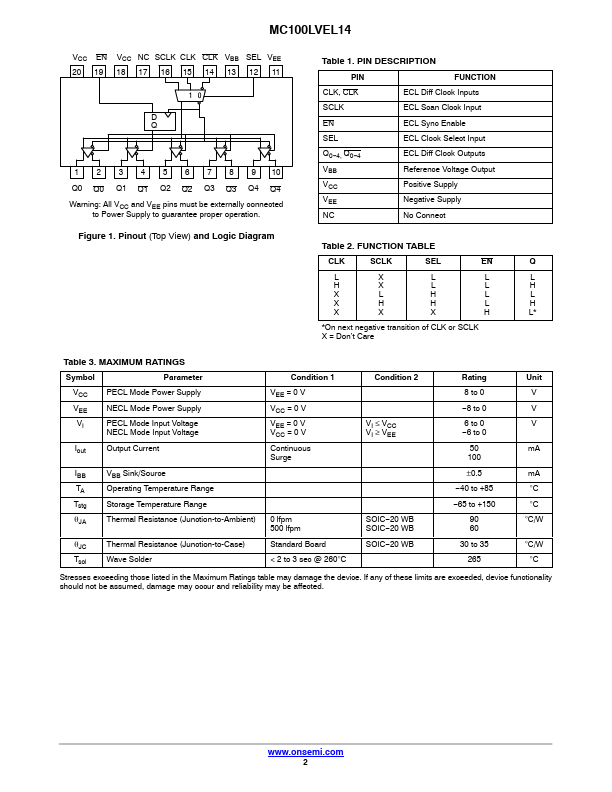
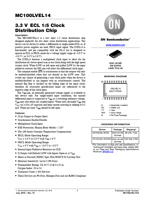
designed explicitly for low skew clock distribution applications.
The device can be driven by either a differential or single-ended ECL or, if positive power supplies are used, PECL input signal.
| Part number | MC100LVEL14 |
|---|---|
| Manufacturer | ON Semiconductor |
| File Size | 138.13 KB |
| Description | 1:5 Clock Distribution Chip |
| Datasheet |
MC100LVEL14 Datasheet
|
|
|
|