Datasheet Details
| Part number | NB3H60113G |
|---|---|
| Manufacturer | ON Semiconductor |
| File Size | 292.65 KB |
| Description | 3.3V / 2.5V Programmable OmniClock Generator |
| Datasheet |
 NB3H60113G-ONSemiconductor.pdf NB3H60113G-ONSemiconductor.pdf
|
| Part number | NB3H60113G |
|---|---|
| Manufacturer | ON Semiconductor |
| File Size | 292.65 KB |
| Description | 3.3V / 2.5V Programmable OmniClock Generator |
| Datasheet |
NB3H60113G-ONSemiconductor.pdf
|
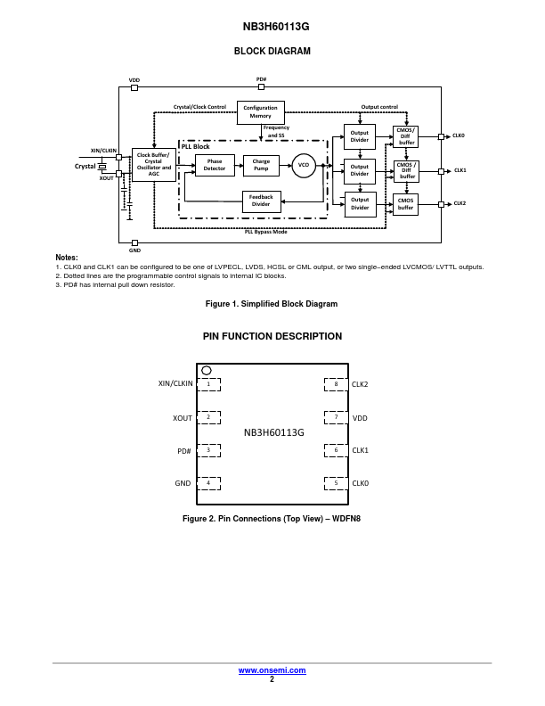
XIN/CLKIN 1 XOUT 2 PD# 3 GND 4 NB3H60113G 8 CLK2 7 VDD 6 CLK1 5 CLK0 Figure 2. Pin Connections (Top View) WDFN8 www.onsemi.com 2 NB3H60113G Table 1. PIN DESCRIPTION Pin No.Pin Name Pin Type 1 XIN/CLKIN Input 2 XOUT Output 3 PD# Input 4 GND Ground 5 CLK0 SE/DIFF output 6 CLK1 SE/DIFF output 7 VDD Power 8 CLK2 SE output Description 3 MHz to 50 MHz crystal input connection or an external single ended reference input clock between 3 MHz and 200 M
📁 NB3H60113G Similar Datasheet