Datasheet Details
- Part number
- NB4L7210
- Manufacturer
- ON Semiconductor ↗
- File Size
- 198.37 KB
- Datasheet
- NB4L7210_ONSemiconductor.pdf
- Description
- 2.5V/3.3V Differential 2x10 Crosspoint Clock Driver
NB4L7210 Description
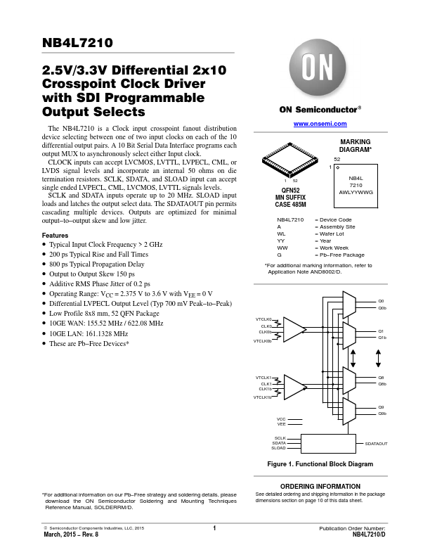
NB4L7210 2.5V/3.3V Differential 2x10 Crosspoint Clock Driver with SDI Programmable Output Selects The NB4L7210 is a Clock input crosspoint fanout dis.
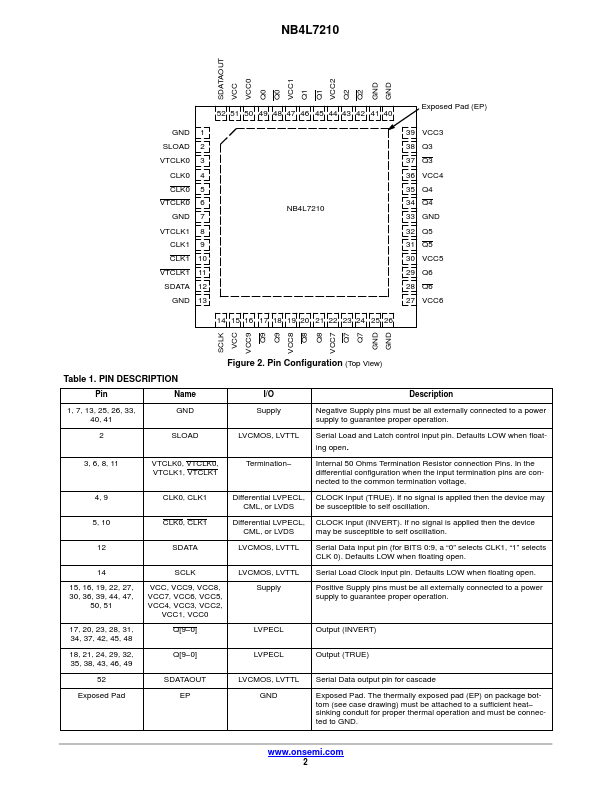
Figure 2.
NB4L7210 Features
* Typical Input Clock Frequency > 2 GHz
* 200 ps Typical Rise and Fall Times
* 800 ps Typical Propagation Delay
* Output to Output Skew 150 ps
* Additive RMS Phase Jitter of 0.2 ps
* Operating Range: VCC = 2.375 V to 3.6 V with VEE = 0 V
* Diff
📁 Related Datasheet
📌 All Tags