Datasheet Details
| Part number | NBXDBA015 |
|---|---|
| Manufacturer | ON Semiconductor |
| File Size | 156.32 KB |
| Description | Clock Oscillator |
| Datasheet |
 NBXDBA015 Datasheet NBXDBA015 Datasheet
|
|
|
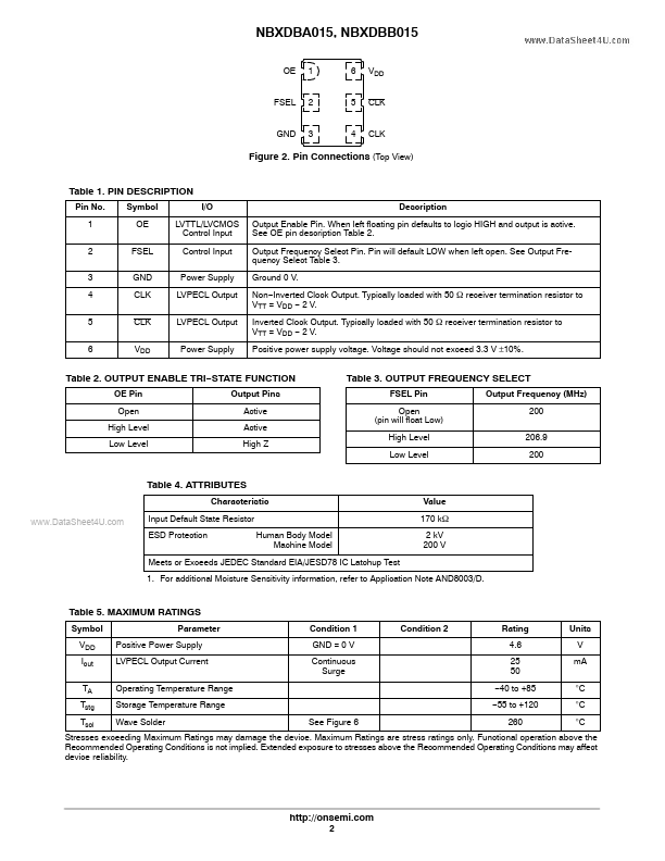
Pin No.
1 2 3 4 5 6 Symbol OE FSEL GND CLK CLK VDD I/O LVTTL/LVCMOS Control Input Control Input Power Supply LVPECL Output LVPECL Output Power Supply Description Output Enable Pin.
When left floating pin defaults to logic HIGH and output is active.
| Part number | NBXDBA015 |
|---|---|
| Manufacturer | ON Semiconductor |
| File Size | 156.32 KB |
| Description | Clock Oscillator |
| Datasheet |
NBXDBA015 Datasheet
|
|
|
|