Description
Pin Name No.
down resistor of 125 kW
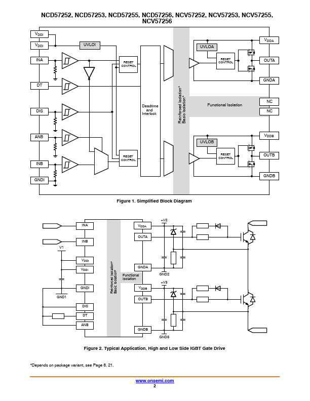
to ensure that output is low in the absence of an input signal.A positive or negative going pulse with pulse width longer than maximum value of tMIN2 is required at INA before OUTA reacts.The input logic levels scale with VDDI up to VDDI = 5 V.With VDDI above 5 V the input logic levels stay the same as for VDDI = 5 V.Maximum
Features
- High Peak Output Current (±6.5 A.
- , ±3.5 A.
- ).
- Configurable as a Dual Low.
- Side or Dual High.
- Side or Half.
- Bridge
Driver.
- Programmable Overlap or Dead Time control.
- Disable Pin to Turn Off Outputs for Power Sequencing.
- ANB Function to Offer Flexibility to Set up the Driver as
Half.
- bridge Driver Operating with a Single Input Signal.
- IGBT/MOSFET Gate Clamping during Short Circuit.
- Short Propagation.
 NCD57252-ONSemiconductor.pdf