Datasheet Details
| Part number | NCV3163 |
|---|---|
| Manufacturer | ON Semiconductor |
| File Size | 239.61 KB |
| Description | Switching Regulator |
| Datasheet |
 NCV3163_ONSemiconductor.pdf NCV3163_ONSemiconductor.pdf
|
| Part number | NCV3163 |
|---|---|
| Manufacturer | ON Semiconductor |
| File Size | 239.61 KB |
| Description | Switching Regulator |
| Datasheet |
NCV3163_ONSemiconductor.pdf
|
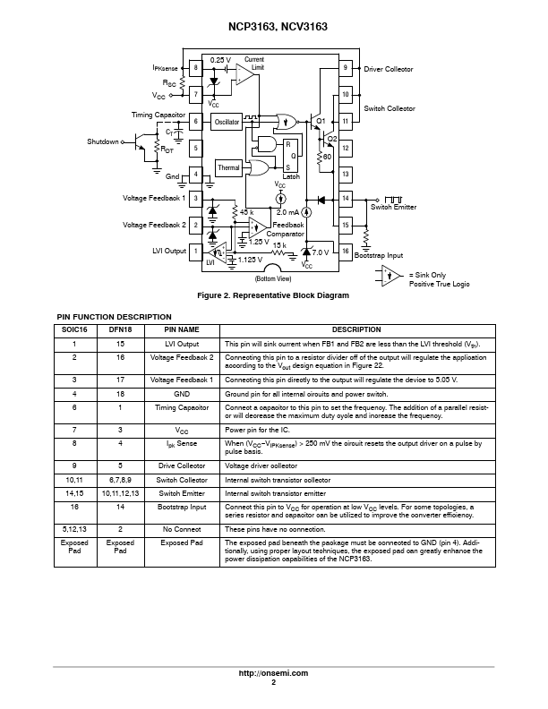
SOIC16 DFN18 PIN NAME 1 15 LVI Output 2 16 Voltage Feedback 2 3 17 Voltage Feedback 1 4 18 GND 6 1 Timing Capacitor 7 8 9 10,11 14,15 16 3 4 5 6,7,8,9 10,11,12,13 14 VCC Ipk Sense Drive Collector Switch Collector Switch Emitter Bootstrap Input 5,12,13 Exposed Pad 2 Exposed Pad No Connect Exposed Pad DESCRIPTION This pin will sink current when FB1 and FB2 are less than the LVI threshold (Vth).Connecting this pin to a resistor divider off of the output will regulate the applicatio
📁 NCV3163 Similar Datasheet