Datasheet Details
| Part number | NCV8665 |
|---|---|
| Manufacturer | ON Semiconductor |
| File Size | 153.35 KB |
| Description | Linear Regulator |
| Datasheet |
 NCV8665_ONSemiconductor.pdf NCV8665_ONSemiconductor.pdf
|
| Part number | NCV8665 |
|---|---|
| Manufacturer | ON Semiconductor |
| File Size | 153.35 KB |
| Description | Linear Regulator |
| Datasheet |
NCV8665_ONSemiconductor.pdf
|
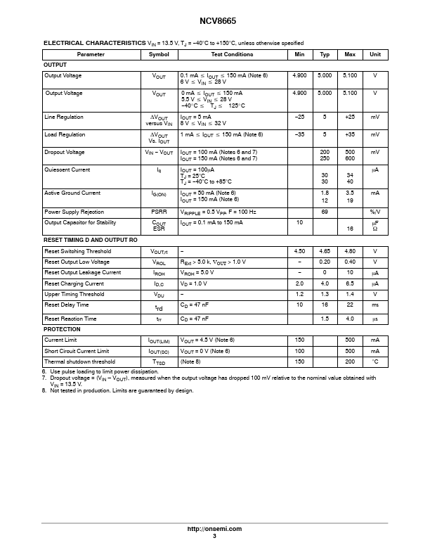
Symbol Function VIN RO GND Unregulated input voltage; 5.5 V to 45 V; Battery Input Voltage.Bypass to GND with a 0.1 mF ceramic capacitor.Reset Output; open collector active Reset (Accurate when VOUT > 1.0 V) Ground; Pin 3 internally connected to Tab D Reset Delay; timing capacitor to GND for Reset Delay function VOUT Output; ±2.0%, 150 mA.10 mF, ESR < 16 W ABSOLUTE MAXIMUM RATINGS Pin Symbol, Parameter Symbol Min Max Unit VIN, DC Input Voltage VOUT, DC Voltage Reset Output Vol
📁 NCV8665 Similar Datasheet