Datasheet Details
| Part number | NCV8851 |
|---|---|
| Manufacturer | ON Semiconductor ↗ |
| File Size | 169.33 KB |
| Description | Automotive Grade Synchronous Buck Controller |
| Datasheet |
 NCV8851_ONSemiconductor.pdf NCV8851_ONSemiconductor.pdf
|
| Part number | NCV8851 |
|---|---|
| Manufacturer | ON Semiconductor ↗ |
| File Size | 169.33 KB |
| Description | Automotive Grade Synchronous Buck Controller |
| Datasheet |
NCV8851_ONSemiconductor.pdf
|
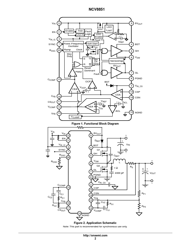
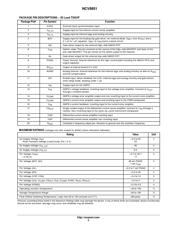
20 Lead TSSOP Package Pin# Pin Symbol Function 1 SYNC External clock synchronization input.2 VIN_CS Supply input for the internal current sense amplifier.3 VIN_IC Supply input for internal logic and analog circuitry.4 BST Supply input for the floating top gate driver.An external diode, DBST, from 6VOUT and a 0.1 mF to 1 mF capacitor, CBST, to VSW forms a boost circuit.5 GH Gate driver output for the external high side NMOS FET. n
📁 NCV8851 Similar Datasheet