Description
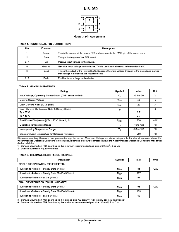
Pin
Function
Description
1
Source
This is the source of the power FET and connects to the PMIC pin of the same name.2
Gate
This pin is the gate of the FET switch.3, 7
Vin
Positive input voltage to the device.4
Ground
Negative input voltage to the device.This is used as the internal reference for the IC.5
Vout
This is the output of the internal LDO.It passes the input voltage through to the output and clamps
that voltage if it exceeds the regulation limit.6, 8
Drain
P
Features
- Lower Power Dissipation and Higher Efficiency vs. Zener Shunt
Regulator.
- LDO Highly Stable across Temperature, Operates Without Bypass
Capacitors.
- Wide 3-30 V Power Supply Voltage Input Range.
- Low.
- Profile (0.75mm) 6-Lead 2x2mm WDFN6 Package.
- This is a Pb.
- Free Device
Typical.
 NIS1050_ONSemiconductor.pdf