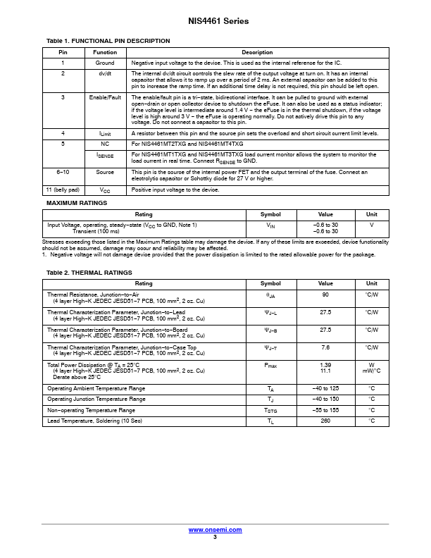
Description
Pin
Function
Description
1
Ground
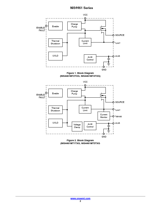
Negative input voltage to the device.This is used as the internal reference for the IC.2
dv/dt
The internal dv/dt circuit controls the slew rate of the output voltage at turn on.It has an internal
capacitor that allows it to ramp up over a period of 2 ms.An external capacitor can be added to this
pin to increase the ramp time.If an additional time delay is not required, this pin should be left open.3
Enable/Fault The enable/fault pin is a tri
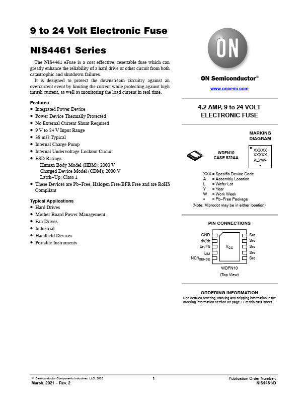
Features
- Integrated Power Device.
- Power Device Thermally Protected.
- No External Current Shunt Required.
- 9 V to 24 V Input Range.
- 39 mW Typical.
- Internal Charge Pump.
- Internal Undervoltage Lockout Circuit.
- ESD Ratings:
Human Body Model (HBM); 2000 V Charged Device Model (CDM); 2000 V Latch.
- Up; Class 1.
- These Devices are Pb.
- Free, Halogen Free/BFR Free and are RoHS
Compliant
Typical.
 NIS4461-ONSemiconductor.pdf