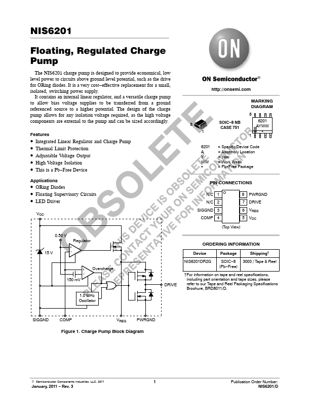
Description
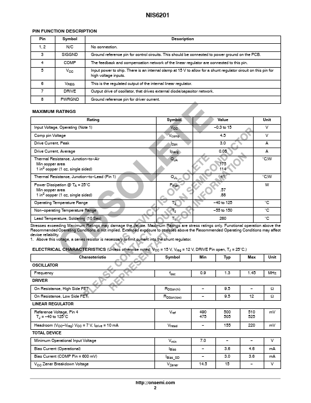
Pin
Symbol
Description
1, 2
N/C
No connection.3
SIGGND
Ground reference pin for control circuits.This should be connected to power ground on the PCB.4
COMP
The feedback and compensation network of the linear regulator are connected to this pin.5
VCC
Input power to chip.There is an internal clamp at 15 V to allow for a shunt regulator circuit on this pin for
high voltage inputs.6
VREG
This is the regulated output of the internal linear regulator.7
DRIVE
Output drive o
Features
- Integrated Linear Regulator and Charge Pump.
- Thermal Limit Protection.
- Adjustable Voltage Output.
- High Voltage Isolation.
- This is a Pb.
- Free Device
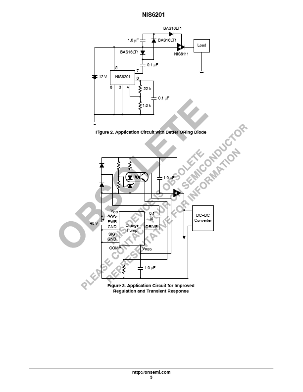
http://onsemi. com
8 1
SOIC.
- 8 NB CASE 751.
 NIS6201_ONSemiconductor.pdf