Datasheet Details
- Part number
- NB3V60113G
- Manufacturer
- ON Semiconductor ↗
- File Size
- 264.84 KB
- Datasheet
- NB3V60113G-ONSemiconductor.pdf
- Description
- 1.8V Programmable OmniClock Generator
NB3V60113G Description
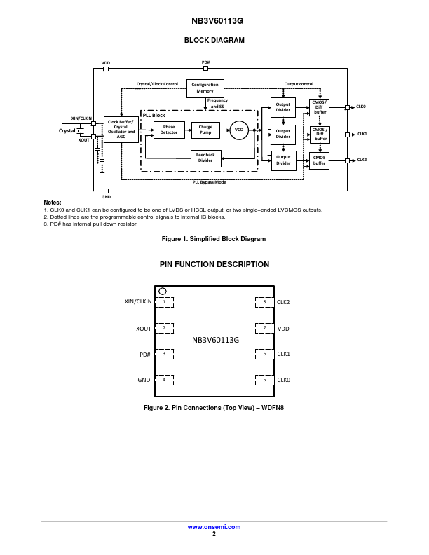
NB3V60113G 1.8 V Programmable OmniClock Generator with Single Ended (LVCMOS) and Differential (LVDS/HCSL) Outputs The NB3V60113G, which is a member.
CLK0 CLK1 CLK2
XIN/CLKIN 1 XOUT 2 PD# 3 GND 4
NB3V60113G
8 CLK2 7 VDD 6 CLK1 5 CLK0
Figure 2.
WDFN8
www.
NB3V60113G Features
* Member of the OmniClock Family of Programmable Clock
Generators
* Operating Power Supply: 1.8 V ± 0.1 V
* I/O Standards
* Inputs: LVCMOS, Fundamental Mode Crystal
* Outputs: LVCMOS
* Outputs: LVDS and HCSL
* 3 Programmable Single Ended (LVCMO
NB3V60113G Applications
* demanding low electromagnetic interference (EMI). Using the PLL bypass mode, it is possible to get a copy of the input clock on any or all of the outputs. The device can be powered down using the Power Down pin (PD#). It is possible to program the internal input crystal load capacitance and the outp
📁 Related Datasheet
📌 All Tags