2SK615
Key Features
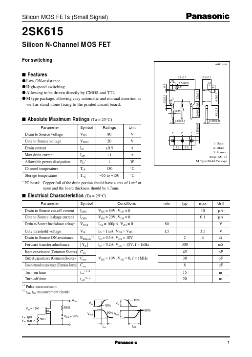
- 9±0.1 1.5 R0.9 R0.9
- 4±0.2 2.0±0.2 3.5±0.1
- 5±0.1 1.0
- 0±0.1 R
- 85 s Absolute Maximum Ratings (Ta = 25°C) Parameter Drain to Source voltage Gate to Source voltage Drain current Max drain current Allowable power dissipation Channel temperature Storage temperature *
- 55±0.1
- 45±0.05
- 25±0.05 Symbol VDS VGSO ID IDP PD * Ratings 80 20 ±0.5 ±1 1 150 -55 to +150 Unit V V A A W °C °C
- 5 2.5 3 2 1 1: Gate 2: Drain 3: Source EIAJ: SC-71 M Type Mold Package Tch Tstg PC board: Copper foil of the drain portion should have a area of 1cm2 or more and the board thickness should be 1.7mm. s Electrical Characteristics (Ta = 25°C) Parameter Drain to Source cut-off current Gate to Source leakage current Drain to Source breakdown voltage Gate threshold voltage Drain to Source ON-resistance Forward transfer admittance Symbol IDSS IGSS VDSS Vth RDS(on) | Yfs | Coss ton*1, 2 toff
- 1, 2 *1 Conditions VDS = 60V, VGS = 0 VGS = 20V, VDS = 0 IDS = 100µA, VGS = 0 ID = 1mA, VDS = VGS ID = 0.5A, VGS = 10V ID = 0.2A, VDS = 15V, f = 1kHz VDS = 10V, VGS = 0, f = 1MHz min typ max 10 0.1