Datasheet Details
- Part number
- AN5491
- Manufacturer
- Panasonic Semiconductor
- File Size
- 69.65 KB
- Datasheet
- AN5491_PanasonicSemiconductor.pdf
- Description
- Synchronous signal and deflection distortion correction processor
AN5491 Description
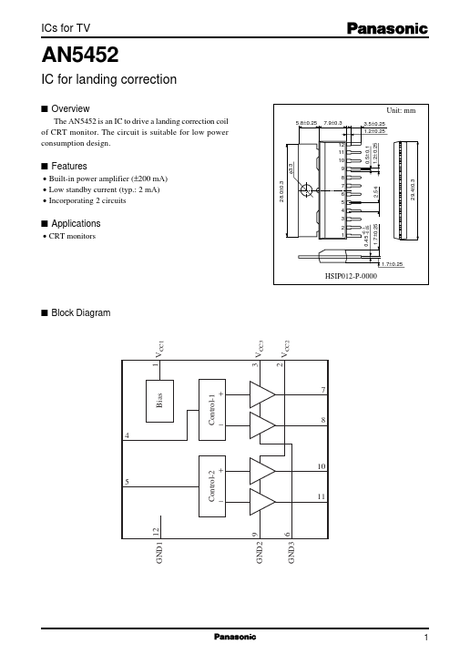
ICs for TV AN5452 IC for landing correction s Overview The AN5452 is an IC to drive a landing correction coil of CRT monitor.The circuit is suitable.
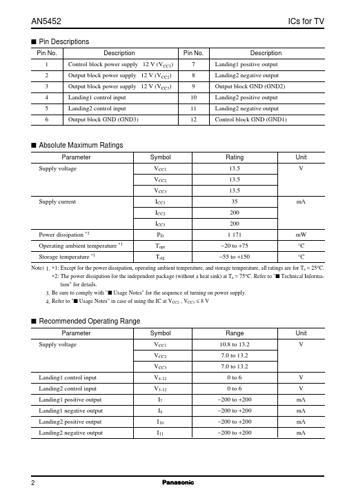
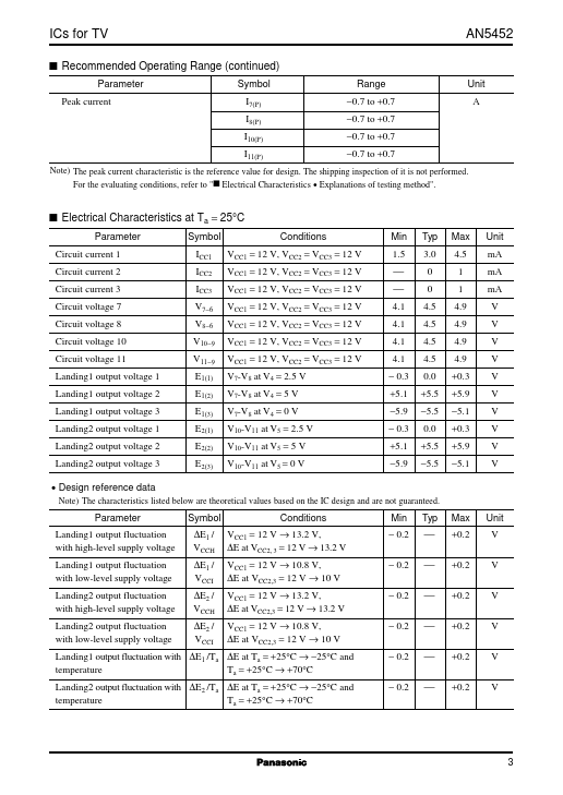
Pin No.
AN5491 Features
* Built-in power amplifier (±200 mA)
* Low standby current (typ. : 2 mA)
* Incorporating 2 circuits
* CRT monitors
+0.1 0.45
AN5491 Applications
* 1.7±0.25
HSIP012-P-0000
s Block Diagram
1 V CC1 3 V CC3 VCC2
2
Bias
Control-1
+
* 7
8
4
5
Control-2
+
📁 Related Datasheet
📌 All Tags