Click to expand full text
WIRELESS, RF, AND CABLE
Jun 01, 2001
TD-SCDMA Radio Chipset Block Diagram for Handset Application
China option for 3G cellular phone is the TD-SCDMA system. A detailed handset transceiver diagram is presented showing MAX2361 as the transmit IC, the MAX2291 as the power amplifier (PA), and the MAX2388 and MAX2309 form the receiver. A VCO buffer amplifier is used to provide isolation and maintains a clean LO signal.
Overview
TD-SCDMA is the third-generation (3G) cellular phone standard currently under development in China. In November 1999, the TD-SCDMA standard was adopted by the ITU as one of the options in the 3GPP mobile communication standard.
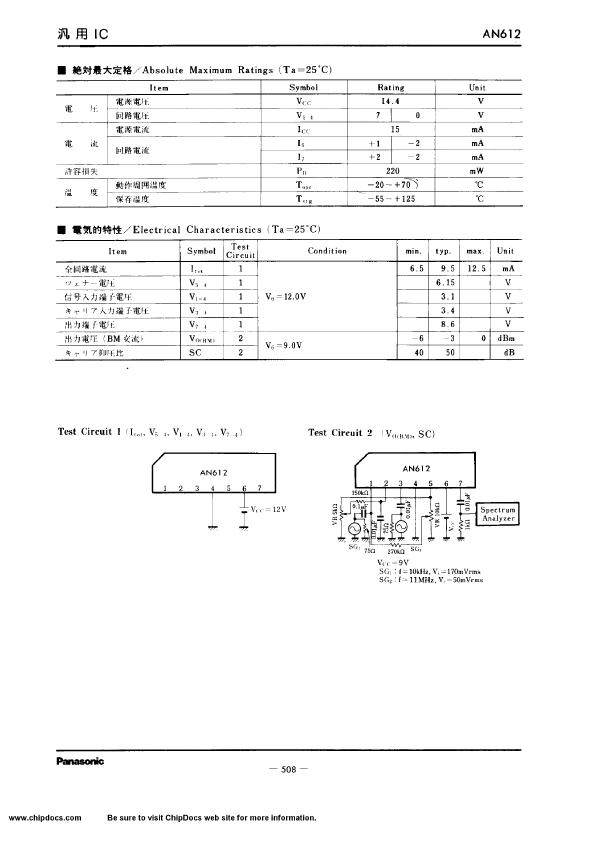
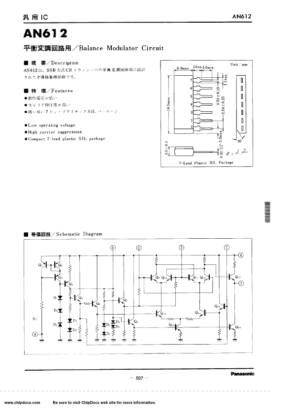
 AN612 Datasheet