Datasheet Details
| Part number | MN195001 |
|---|---|
| Manufacturer | Panasonic Semiconductor |
| File Size | 83.57 KB |
| Description | Single-Chip Fax Engine LSI |
| Datasheet |
 MN195001_PanasonicSemiconductor.pdf MN195001_PanasonicSemiconductor.pdf
|
| Part number | MN195001 |
|---|---|
| Manufacturer | Panasonic Semiconductor |
| File Size | 83.57 KB |
| Description | Single-Chip Fax Engine LSI |
| Datasheet |
MN195001_PanasonicSemiconductor.pdf
|
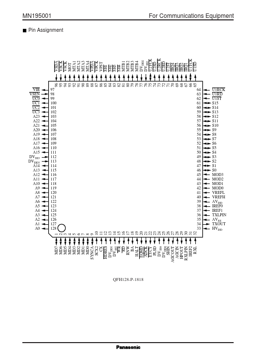
Functional Group For Communications Equipment Symbol A0 to 23 MD0 to 7 RD WR R/W CX SCX2 SYNCA HDRES MOD0 to 3 HALT BA IREF0 IREF1 TXLPIN TXOUT RXL IREF2 RXLPIN HPOUT AGCIN AGCOUT SHIN VREFH VREFL PLSD SO to 15 UC0 to 3 IRO1 to 4 U1ST U1RD U1RCK U1SD U1TCK U2ST U2RD U2RCK U2SD U2TCK SH1 to 4 MTA1 to 4 Pin No.128 to 114, 111 to 103 8 to 1 16 15 17 11 10 9 12 42 to 45 19 18 38 37 36 34 32 31 30 29 28 27 26 40 41 23 46 to 61 99 to 102 67 to 70 62 63 64 65 66 71 72 73 74 75 85 to 82 92 to 89 I
📁 MN195001 Similar Datasheet