Datasheet4U Logo Datasheet4U.com

MN3307 Datasheet - Panasonic Semiconductor

MN3307_PanasonicSemiconductor.pdf
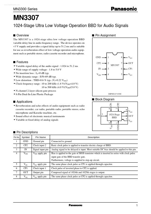
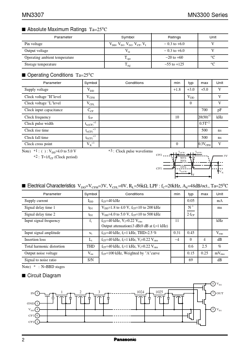
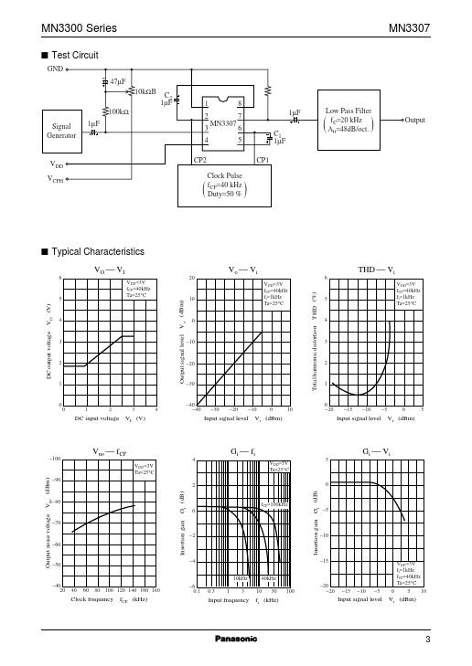
Preview of MN3307 PDF
MN3307 Datasheet Preview Page 2 MN3307 Datasheet Preview Page 3

Datasheet Details

Part number:

MN3307

Manufacturer:

Panasonic Semiconductor

File Size:

86.09 KB

Description:

1024-stage ultra low voltage operation bbd.

MN3307, 1024-Stage Ultra Low Voltage Operation BBD

Pin No.

Symbol 1 2 3 4 GND CP2 IN VDD Pin Name Ground pin Clock input 2 Signal input pin VDD apply pin Connected to ground.

Basic clock pulse is applied to transfer electric charge of BBD.

Analog signal to be delayed is input.

Most suitable DC bias should be applied to this pin.

Bias is applied to

www.DataSheet4U.com MN3300 Series MN3307 1024-Stage Ultra Low Voltage Operation BBD for Audio Signals s Overview The MN3307 is a 1024-stage ultra low voltage operation BBD variable delay line in audio frequency range.

The device operates on +3 V supply and provides a signal delay up to 51.2 ms and is suitable for use as reverberation effect of low voltage operation audio equipment such as portable stereo, radio cassette recorder and microphone.

GND 1 2 MN3307 IN VDD 3 4 6 5 CP1 VD1 8 7 VD2 OUT

MN3307 Features

* Variable signal delay of the audio signal : 1.024 to 51.2 ms

* Wide range of supply voltage : 1.8 to 5.0 V

* No insertion loss : Li=0 dB typ.

* Wide dynamic range : S/N=69 dB typ.

* Low distortion : THD=0.6 % typ. (Vi=0.22 Vrms)

* Clock frequency ran

📁 Related Datasheet

📌 All Tags

Panasonic Semiconductor MN3307-like datasheet