Description
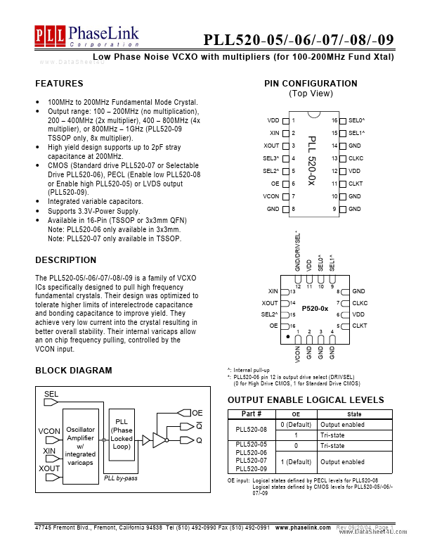
11
SEL1^
9
8 7 6 5
GND CLKC VDD CLKT
P520-0x
2 3 4
PLL520-05/-06/-07/-08/-09
www.DataSheet4U.com
Low Phase Noise VCXO with multipliers (for 100-200MHz Fund Xtal)
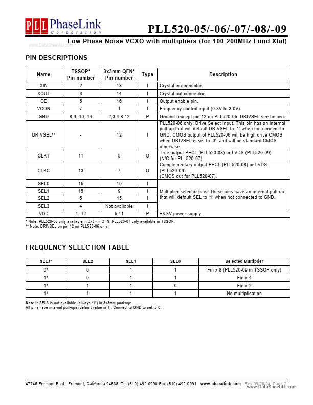
PIN DESCRIPTIONS
Name
XIN XOUT OE VCON GND DRIVSEL
TSSOP
Pin number
2 3 6 7 8,9, 10, 14 -
3x3mm QFN
Pin number
13 14 16 1 2,3,4,8,12 12
Type
I I I I P I
Description
Crystal in connector.Crystal out connector.Output enable pin.Frequency control input (0.3V to 3.0V) Ground (except pin 12 on PLL520-06: DR
Features
- 100MHz to 200MHz Fundamental Mode Crystal. Output range: 100.
- 200MHz (no multiplication), 200.
- 400MHz (2x multiplier), 400.
- 800MHz (4x multiplier), or 800MHz.
- 1GHz (PLL520-09 TSSOP only, 8x multiplier). High yield design supports up to 2pF stray capacitance at 200MHz. CMOS (Standard drive PLL520-07 or Selectable Drive PLL520-06), PECL (Enable low PLL520-08 or Enable high PLL520-05) or LVDS output (PLL520-09). Integrated variable capacitors.
 PLL520-05_PhaseLinkCorporation.pdf