PPMT2301
Description
- Trench Power LV MOSFET technology
- High Power and Current handing capability
- Low Gate Charge
MOSFET Product Summary
VDS(V) -20
RDS(on)(mΩ) 90@VGS = -4.5V 135@VGS = -2.5V
ID(A) -4.0
Applications
- PWM applications
- Load switch
- Power management
PPMT2301 P-Channel MOSFET
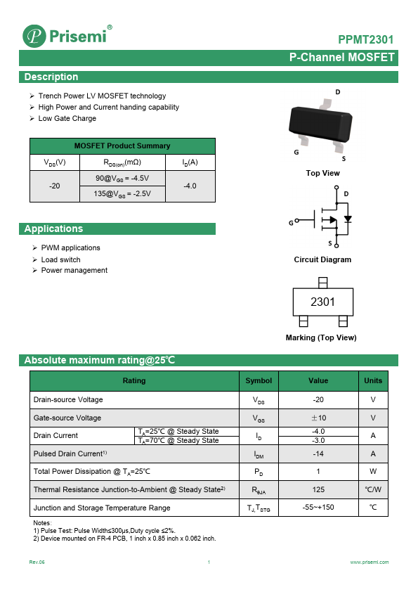
Top View
Circuit Diagram
Absolute maximum rating@25℃
Rating
Drain-source Voltage
Gate-source Voltage Drain Current Pulsed Drain Current1)
TA=25℃ @ Steady State TA=70℃ @ Steady State
Total Power Dissipation @ TA=25℃ Thermal Resistance Junction-to-Ambient @ Steady State2)
Junction and Storage Temperature Range
Notes: 1) Pulse Test: Pulse Width≤300μs,Duty cycle ≤2%. 2) Device mounted on FR-4 PCB, 1 inch x 0.85 inch x 0.062 inch.
Rev.06
Marking (Top View)
Symbol
VDS VGS ID IDM PD RθJA TJ,TSTG
Value
-20
±10 -4.0 -3.0 -14
-55~+150
Units V V A A W
℃/W ℃
.prisemi.
P-Channel MOSFET
Electrical characteristics per line@25℃ (unless otherwise...