PPMT2307 Overview
Description
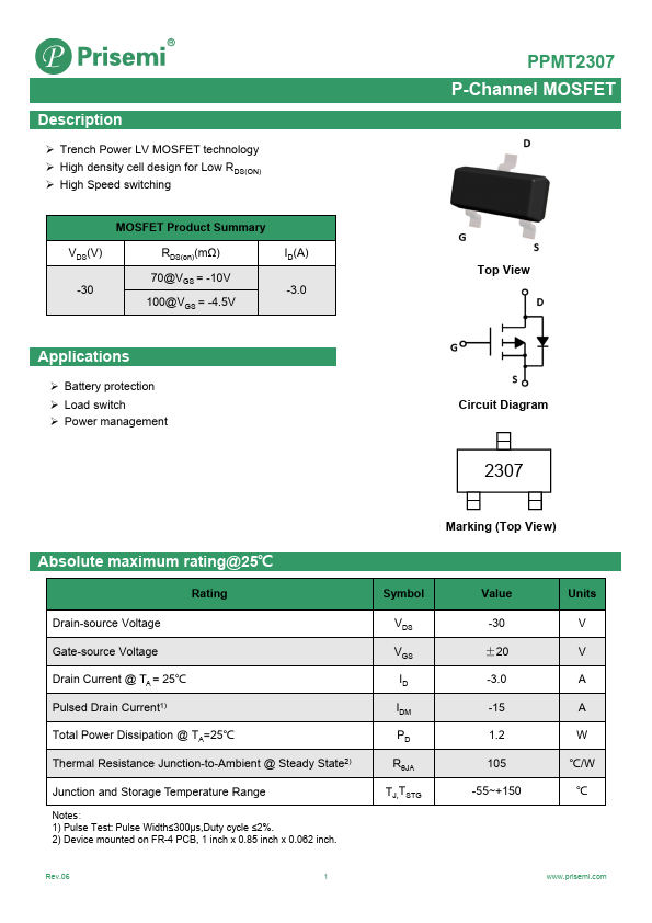
Trench Power LV MOSFET technology - High density cell design for Low RDS(ON) - High Speed switching MOSFET Product Summary VDS(V) -30 RDS(on)(mΩ) 70@VGS = -10V 100@VGS = -4.5V ID(A) -3.0.
| Part | PPMT2307 |
|---|---|
| Description | P-Channel MOSFET |
| Category | MOSFET |
| Manufacturer | Prisemi |
| Size | 1.13 MB |
Trench Power LV MOSFET technology - High density cell design for Low RDS(ON) - High Speed switching MOSFET Product Summary VDS(V) -30 RDS(on)(mΩ) 70@VGS = -10V 100@VGS = -4.5V ID(A) -3.0.
| Part Number | Manufacturer | Description |
|---|---|---|
| A2SHB | HAOHAI | N-Channel MOSFET |
| AP9563GH | Advanced Power Electronics Corp | P-CHANNEL ENHANCEMENT MODE POWER MOSFET |
| FCPF360N65S3R0L | onsemi | N-Channel MOSFET |