Datasheet Details
| Part number | HD74LV2G126A |
|---|---|
| Manufacturer | Renesas Technology |
| File Size | 127.36 KB |
| Description | Dual Bus Buffer |
| Datasheet |
 HD74LV2G126A Datasheet HD74LV2G126A Datasheet
|
|
|
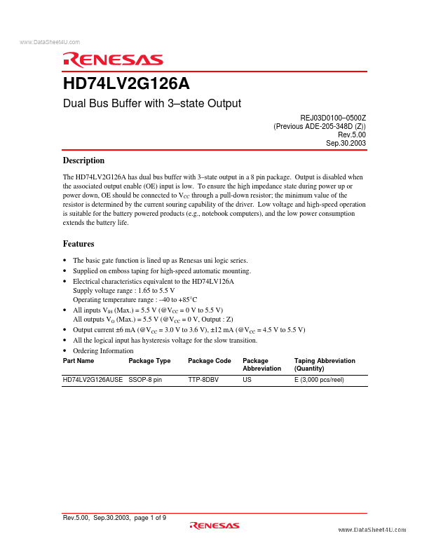
state output in a 8 pin package.
Output is disabled when the associated output enable (OE) input is low.
| Part number | HD74LV2G126A |
|---|---|
| Manufacturer | Renesas Technology |
| File Size | 127.36 KB |
| Description | Dual Bus Buffer |
| Datasheet |
HD74LV2G126A Datasheet
|
|
|
|