Datasheet4U Logo Datasheet4U.com

82C89 - CMOS Bus Arbiter

📥 Download Datasheet

Preview of 82C89 PDF
datasheet Preview Page 2 datasheet Preview Page 3

82C89 Product details

Description

PIN SYMBOL NUMBER TYPE DESCRIPTION VCC GND 20 10 
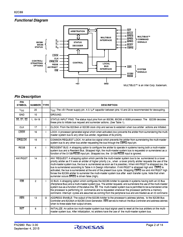
VCC: The +5V Power supply pin.A 0.1F capacitor between pins 10 and 20 is recommended for decoupling.GROUND.S0, S1, S2 1, 18-19 I STATUS INPUT PINS: The status input pins from an 80C86, 80C88 or 8089 processor.The 82C89 decodes these pins to initiate bus request and surrender actions.(See Table 1).CLK 17 I CLOCK: From the 82C84A or 82C85 clock chip and serves to establish when bus arbiter actions are initiated.LOCK 16 I LOCK: A pr

Features

📁 82C89 Similar Datasheet

  • 82C895 - System / Power Management Controller (Opti)
  • 82C802G - System / Power Management Controller (Opti)
  • 82C802GP - System / Power Management Controller (Opti)
  • 82C814 - Docking Station Controller Preliminary Data Book (Opti)
  • 82C82 - CMOS Octal Latching Bus Driver (Intersil Corporation)
  • 82C836 - Single-Chip 386sx AT (Chips)
  • 82C83H - CMOS Octal Latching Inverting Bus Driver (Intersil Corporation)
  • 82C84A - CMOS Clock Generator Driver (Intersil Corporation)
Other Datasheets by Renesas
Published: |