Datasheet Details
| Part number | R5F56104WNBG |
|---|---|
| Manufacturer | Renesas |
| File Size | 1.13 MB |
| Description | 32-Bit MCU |
| Datasheet |
|
|
|
|
Download the R5F56104WNBG datasheet PDF. This datasheet also includes the R5F56108VNFP variant, as both parts are published together in a single manufacturer document.
| Part number | R5F56104WNBG |
|---|---|
| Manufacturer | Renesas |
| File Size | 1.13 MB |
| Description | 32-Bit MCU |
| Datasheet |
|
|
|
|
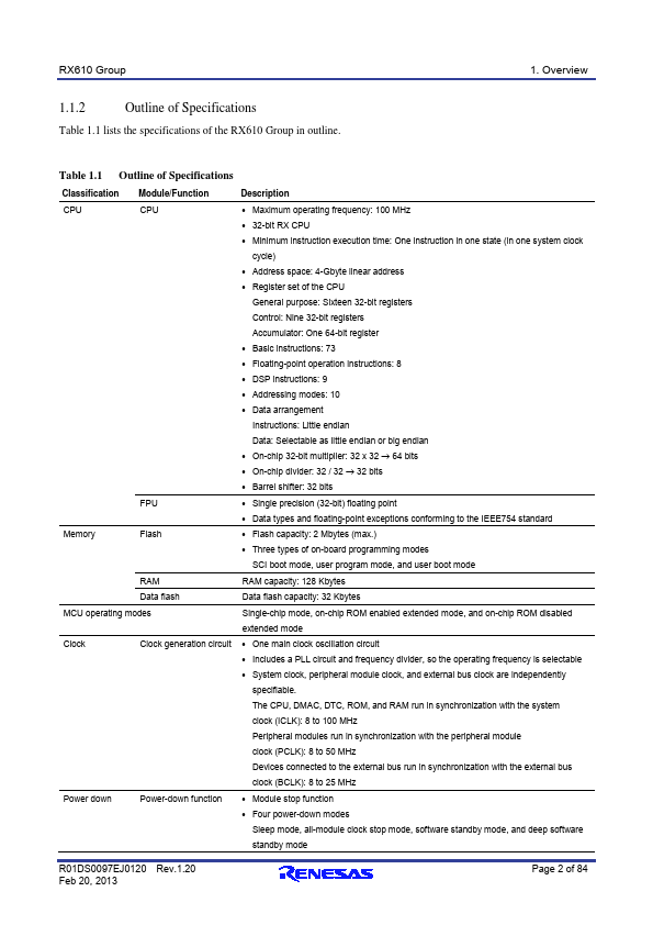
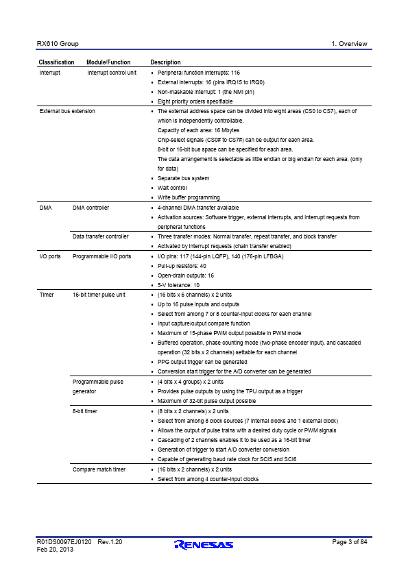
CPU CPU Memory FPU Flash RAM Data flash MCU operating modes Clock Clock generation circuit Power down Power-down function • Maximum operating frequency: 100 MHz • 32-bit RX CPU • Minimum instruction execution time: One instruction in one state (in one system clock cycle) • Address space: 4-Gbyte linear address • Register set of the CPU General purpose: Sixteen 32-bit registers Control: Nine 32-bit registers Accumulator: One 64-bit register • Basic instructions: 73 • Floating-point operation instructions: 8 • DSP instructions: 9 • Addressing modes: 10 • Data arrangement Instructions: Little endian D
Datasheet RX610 Group Datasheet RENESAS 32-Bit MCU R01DS0097EJ0120 Rev.1.20 Feb 20, 2013 1.
Overview 1.
| Part Number | Description |
|---|---|
| R5F56104WDBG | 32-Bit MCU |
| R5F56104VDFP | 32-Bit MCU |
| R5F56104VNFP | 32-Bit MCU |
| R5F56106VDFP | 32-Bit MCU |
| R5F56106VNFP | 32-Bit MCU |
| R5F56106WDBG | 32-Bit MCU |
| R5F56106WNBG | 32-Bit MCU |
| R5F56107VDFP | 32-Bit MCU |
| R5F56107VNFP | 32-Bit MCU |
| R5F56107WDBG | 32-Bit MCU |