Description
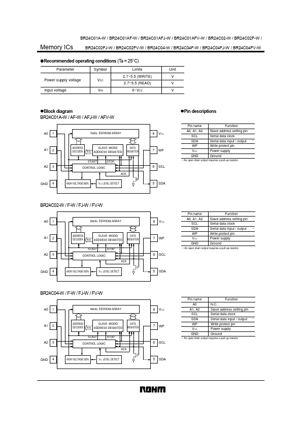
Pin name A0, A1, A2 SCL SDA WP VCC GND Function Slave address setting pin Serial data clock Serial data input / output Write protect pin Power supply Ground
A0
1
7bits
1kbits EEPROM ARRAY
8bits
8
VCC
∗
A1
2
ADDRESS DECODER
7bits
SLAVE
WORD ADDRESS REGISTER
DATA REGISTER
7
WP
START
STOP
∗ An open drain output requires a pull-up resistor.A2
3
CONTROL LOGIC ACK
6
SCL
GND
4
HIGH VOLTAGE GEN.VCC LEVEL DETECT
5
SDA
BR24C02-W / F-W / FJ-W / FV-W
Pin name A0, A1, A2
Features
- 1) 128×8bits (1k) serial EEPROM. (BR24C01A-W / AF-W / AFJ-W / AFV-W) 256×8bits (2k) serial EEPROM. (BR24C02-W / F-W / FJ-W / FV-W) 512×8bits (4k) serial EEPROM. (BR24C04-W / F-W / FJ-W / FV-W) 2) Two wire serial interface. 3) Operating voltage range : 2.7V∼5.5V 4) Low current consumption Active (at 5V) : 1.5mA (Typ. ) Standby (at 5V) : 0.1µA (Typ. ) 5) Auto erase and auto complete functions can be used during write operations. 6) Page write function. BR24C01A-W / AF-W / AFJ-W / AFV-W : 8 bytes BR.
 BR2-4C0.pdf