74107
74107 is DUAL J-K FLIP-FLOP manufactured by STMicroelectronics.
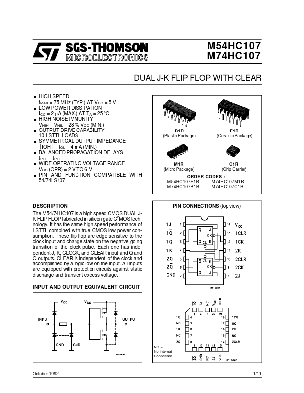
PTION The M54/74HC107 is a high speed CMOS DUAL JK FLIP FLOP fabricated in silicon gate C2MOS technology. It has the same high speed performance of LSTTL bined with true CMOS low power consumption. These flip-flop are edge sensitive to the clock input and change state on the negative going transition of the clock pulse. Each one has independent J, K, CLOCK, and CLEAR input and Q and Q outputs. CLEAR is independent of the clock and acplished by a logic low on the input. All inputs are equipped with protection circuits against static discharge and transient excess voltage. INPUT AND OUTPUT EQUIVALENT CIRCUIT
PIN CONNECTIONS (top view)
NC = No Internal Connection
October 1992
1/11
M54/M74HC107
TRUTH TABLE
INPUTS CLR L H H H H H
X: Don’t Care
OUTPUTS K X L H L H X CK X Q L Qn L H Qn Qn Q H Qn H L Qn Qn
J X L L H H X
FUNCTION CLEAR NO CHANGE
TOGGLE NO CHANGE
PIN DESCRIPTION
PIN No 1, 8, 4, 11 2, 6 3, 5 12, 9 13, 10 7 14 SYMBOL 1J, 2J, 1K, 2K 1Q, 2Q 1Q, 2Q 1CK, 2CK 1CLR, 2CLR GND V CC NAME AND FUNCTION Synchronous Inputs; Flip-Flop 1 And 2 plement Flip-Flop Outputs True Flip-Flop Outputs Clock Input Asynchronous Reset Inputs Ground (0V) Positive Supply Voltage
IEC LOGIC SYMBOL
LOGIC DIAGRAM (1/2 Package)
2/11
M54/M74HC107
ABSOLUTE MAXIMUM RATINGS
Symbol VCC VI VO IIK IOK IO ICC or IGND PD Tstg Supply Voltage DC Input Voltage DC Output Voltage DC Input Diode Current DC Output Diode Current DC Output Source Sink Current Per Output Pin DC VCC or Ground Current Power Dissipation Storage Temperature Parameter Value -0.5 to +7 -0.5 to VDD + 0.5 -0.5 to VDD + 0.5 ± 20 ± 20 ± 25 ± 50 500 (- ) -65 to +150 Unit V V V m A m A m A m A m W o
Absolute Maximum Ratings are those values beyond which damage to the device may occur. Functional operation under these condition isnotimplied. (- ) 500 m W: ≅ 65 o C derate to 300 m W by 10m W/o C: 65 o C to 85 o C
REMENDED OPERATING CONDITIONS
Symbol VCC VI VO Top tr, tf Parameter Supply Voltage Input Voltage Output Voltage Operating...