Click to expand full text
www.DataSheet4U.com
DDR SDRAM stacked 1Gb B-die (x4/x8)
DDR SDRAM
Stacked 1Gb B-die DDR SDRAM Specification (x4/x8) Revision 1.1
Rev. 1.1 August. 2003
www.DataSheet4U.com
DDR SDRAM stacked 1Gb B-die (x4/x8)
st. 1Gb B-die Revision History
Revision 0.0 (May, 2003) - First version for internal review. Revision 1.0 (June, 2003) - Deleted "B3" speed. Revision 1.1 (August, 2003) - Corrected typo.
DDR SDRAM
Rev. 1.1 August. 2003
www.DataSheet4U.com
DDR SDRAM stacked 1Gb B-die (x4/x8)
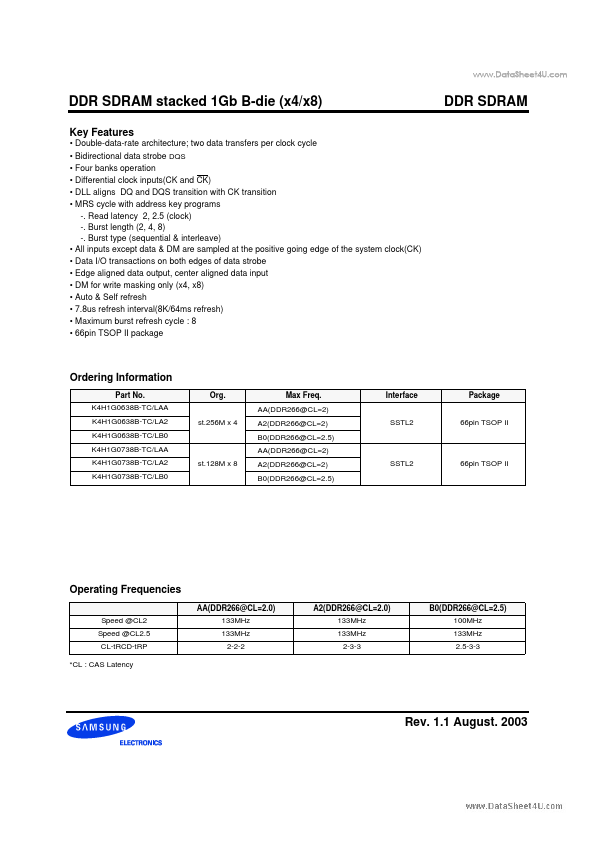
Key Features
• Double-data-rate architecture; two data transfers per clock cycle • Bidirectional data strobe DQS • Four banks operation • Differential clock inputs(CK and CK) • DLL aligns DQ and DQS transition with CK transition • MRS cycle with address key programs -. Read latency 2, 2.5 (clock) -.
 K4H1G0738B Datasheet