Datasheet Details
| Part number | 8531X01 |
|---|---|
| Manufacturer | Samsung semiconductor |
| File Size | 189.93 KB |
| Description | S1T8531X01 |
| Datasheet |
 8531X01_Samsungsemiconductor.pdf 8531X01_Samsungsemiconductor.pdf
|
| Part number | 8531X01 |
|---|---|
| Manufacturer | Samsung semiconductor |
| File Size | 189.93 KB |
| Description | S1T8531X01 |
| Datasheet |
8531X01_Samsungsemiconductor.pdf
|
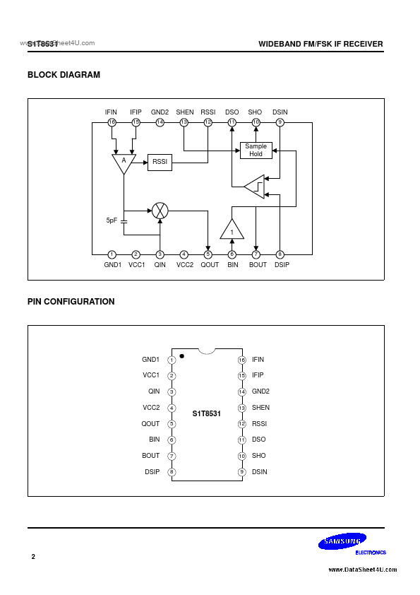
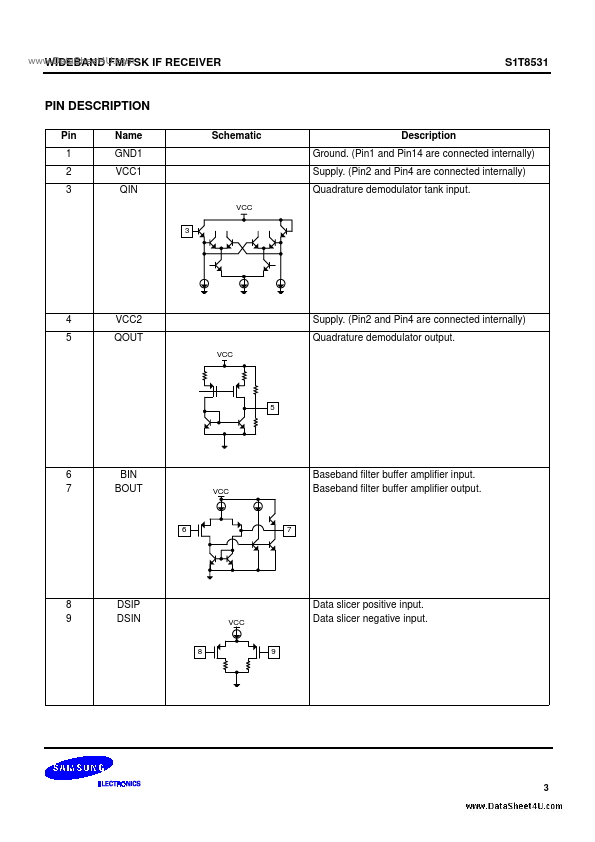
Pin 1 2 3 Name GND1 VCC1 QIN VCC 3 Schematic Description Ground.(Pin1 and Pin14 are connected internally) Supply.(Pin2 and Pin4 are connected internally) Quadrature demodulator tank input.4 5 VCC2 QOUT VCC Supply.(Pin2 and Pin4 are connected internally) Quadrature demodulator output.5 6 7 BIN BOUT VCC Baseband filter buffer amplifier input.Baseband filter buffer amplifier output.6 7 8 9 DSIP DSIN 8 VCC Data slicer positive input.Data slicer negative input.9 3 www.DataS
📁 8531X01 Similar Datasheet