Click to expand full text
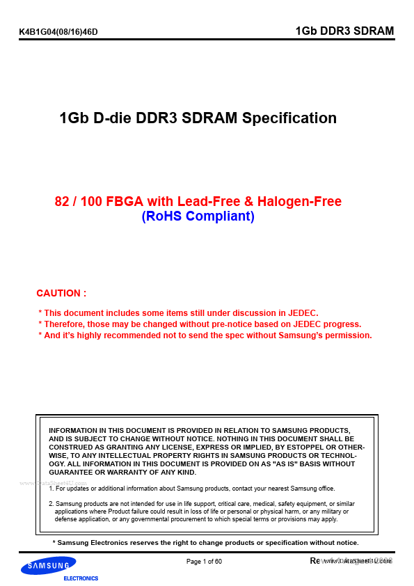
K4B1G04(08/16)46D
1Gb DDR3 SDRAM
1Gb D-die DDR3 SDRAM Specification
82 / 100 FBGA with Lead-Free & Halogen-Free (RoHS Compliant)
CAUTION :
* This document includes some items still under discussion in JEDEC. * Therefore, those may be changed without pre-notice based on JEDEC progress. * And it’s highly recommended not to send the spec without Samsung’s permission.
INFORMATION IN THIS DOCUMENT IS PROVIDED IN RELATION TO SAMSUNG PRODUCTS, AND IS SUBJECT TO CHANGE WITHOUT NOTICE. NOTHING IN THIS DOCUMENT SHALL BE CONSTRUED AS GRANTING ANY LICENSE, EXPRESS OR IMPLIED, BY ESTOPPEL OR OTHERWISE, TO ANY INTELLECTUAL PROPERTY RIGHTS IN SAMSUNG PRODUCTS OR TECHNOLOGY. ALL INFORMATION IN THIS DOCUMENT IS PROVIDED ON AS "AS IS" BASIS WITHOUT GUARANTEE OR WARRANTY OF ANY KIND.
www.DataSheet4U.
 K4B1G0846D Datasheet