Description
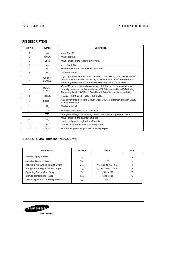
Pin No 1 2 3 4 5 6 Symbol VBB GNDA VFRO VCC FSR DR BCLKR / CLKSEL MCLKR / PDN MCLKX BCLKX DX FSX TSX GSX VFXI VFXI
+
Description VBB = - 5V ±5%.Analog ground.Analog output of the receive power Amp.VCC = +5V ± 5%.Receive frame sync pulse.8KHz pulse train.PCM data input.Logic input which selects either 1.536MHz/1.544MHz or 2.048MHz for master clock in normal operation and BCLKX is used for both TX and RX directions.Alternately direct clock input available, very from 64KHz to 2.048MHz.Whe
Features
- Complete CODEC and filtering system.
- Meets or exceeds AT&T D3/D4 and CCITT specifications µ-Law : KT8554B, A-Law : KT8557B.
- On-chip auto zero, sample and hold, and precision voltage references.
- Low power dissipation : 60mW (operating) 3mW (standby).
- ± 5V operation.
- TTL or CMOS compatible.
- Automatic power down
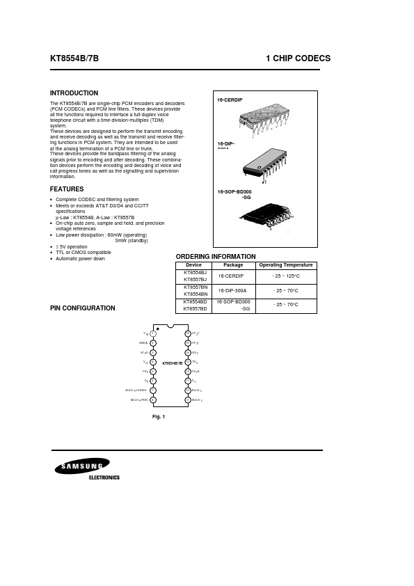
16-SOP-BD300 -SG.
 KT8554 Datasheet