Datasheet Details
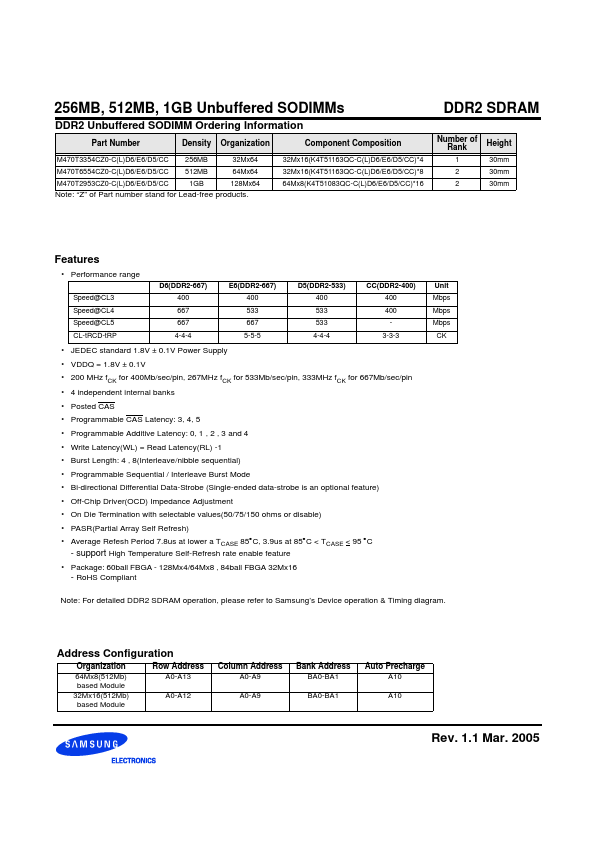
| Part number | M470T6554CZ0 |
|---|---|
| Manufacturer | Samsung semiconductor |
| File Size | 270.34 KB |
| Description | DDR2 Unbuffered SODIMM |
| Datasheet |
 M470T6554CZ0_Samsungsemiconductor.pdf M470T6554CZ0_Samsungsemiconductor.pdf
|
| Part number | M470T6554CZ0 |
|---|---|
| Manufacturer | Samsung semiconductor |
| File Size | 270.34 KB |
| Description | DDR2 Unbuffered SODIMM |
| Datasheet |
M470T6554CZ0_Samsungsemiconductor.pdf
|
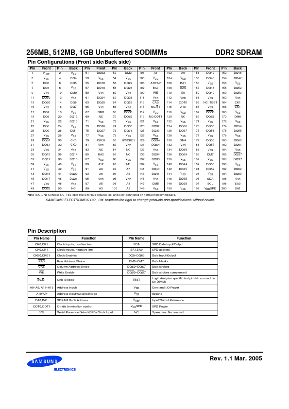
Pin Name CK0,CK1 CK0,CK1 CKE0,CKE1 RAS CAS WE S0,S1 A0~A9, A11~A13 A10/AP BA0,BA1 ODT0,ODT1 SCL Function Clock Inputs, positive line Clock Inputs, negative line Clock Enables Row Address Strobe Column Address Strobe Write Enable Chip Selects Address Inputs Address Input/Autoprecharge SDRAM Bank Address On-die termination control Serial Presence Detect(SPD) Clock Input Pin Name SDA SA1,SA0 DQ0~DQ63 DM0~DM7 DQS0~DQS7 DQS0~DQS7 TEST VDD VSS VREF VDDSPD NC SPD address Data Input/Output Data Masks
📁 M470T6554CZ0 Similar Datasheet