Datasheet Details
| Part number | M383L6423ETS |
|---|---|
| Manufacturer | Samsung |
| File Size | 448.79 KB |
| Description | DDR SDRAM Registered Module |
| Datasheet |
 M383L6423ETS_Samsungsemiconductor.pdf M383L6423ETS_Samsungsemiconductor.pdf
|
|
|
The M383L6423ETS by Samsung is a DDR SDRAM Registered Module. Below is the official datasheet preview.
| Part number | M383L6423ETS |
|---|---|
| Manufacturer | Samsung |
| File Size | 448.79 KB |
| Description | DDR SDRAM Registered Module |
| Datasheet |
M383L6423ETS_Samsungsemiconductor.pdf
|
|
|
|
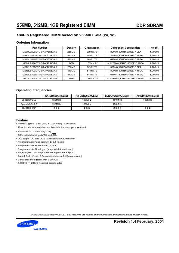
Pin Name A0 ~ A12 BA0 ~ BA1 DQ0 ~ DQ63 DQS0 ~ DQS17 CK0,CK0 ~ CK2, CK2 CKE0, CKE1(for double banks) CS0, CS1(for double banks) RAS CAS WE CB0 ~ CB7 Function Address input (Multiplexed) Bank Select Address Data input/output Data Strobe input/output Clock input Clock enable input Chip select input Row address strobe Column address strobe Write enable Check bit(Data-in/data-out) Pin Name DM0 ~ DM8 VDD VDDQ VSS VREF VDDSPD SDA SCL SA0 ~ 2 NC Data - in mask Power supply (2.5V) Power Supply for DQS(2.
📁 M383L6423ETS Similar Datasheet