Si2301
FEATURES
Super high dense cell design for low RDS(ON) Rugged and reliable Simple drive requirement SOT-23 package
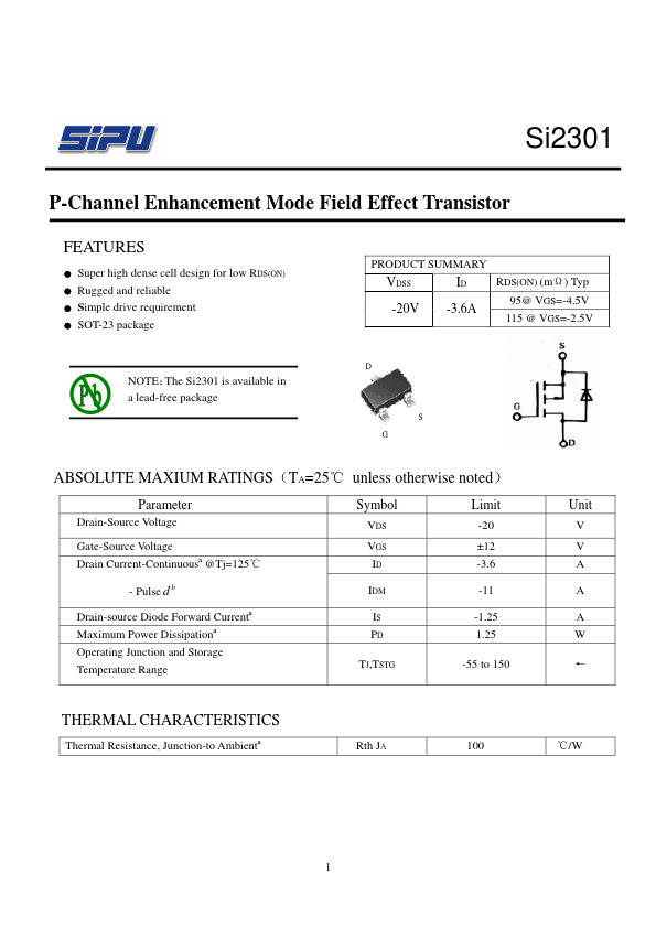
PRODUCT SUMMARY
VDSS
ID RDS(ON) (m ) Typ
-20V
-3.6A
95@ VGS=-4.5V 115 @ VGS=-2.5V
NOTE The Si2301 is available in a lead-free package
ABSOLUTE MAXIUM RATINGS TA=25
Parameter
Drain-Source Voltage
Gate-Source Voltage Drain Current-Continuousª@Tj=125
- Pulse d b
Drain-source Diode Forward Currentª Maximum Power Dissipationª Operating Junction and Storage Temperature Range unless otherwise noted
Symbol
VDS VGS ID
Limit
-20 ±12 -3.6
IDM -11
IS -1.25 PD 1.25
TJ,TSTG
-55 to 150
Unit
THERMAL CHARACTERISTICS
Thermal Resistance, Junction-to Ambientª
Rth JA
/W
ELECTRICAL CHARACTERISTICS (TA=25 unless otherwise noted)
Parameter
OFF CHARACTERISTICS Drain-Source Breakdown Voltage Zero Gate Voltage Drain Current Gate-Body Leakage
ON CHARACTERITICS
Gate Threshold Voltage
Drain-Source On-State Resistance
Forward Transconductance...