Datasheet4U Logo Datasheet4U.com

HYS64V4120GU-10 - 3.3V 4M x 64-Bit 2 BANK SDRAM Module 3.3V 4M x 72-Bit 2 BANK SDRAM Module

Description

A0-A10 BS (A11) DQ0 - DQ63 CB0-CB7 RAS CAS WE CKE0, CKE1 CLK0 - CLK3 DQMB0 - DQMB7 CS0 - CS3 Vcc Vss SCL SDA N.C.

Features

  • s are registered on every rising clock edge during tRC(min). Values are shown per module bank. 2. The specified values are valid when data inputs (DQ’ s) are stable during tRC(min. ). 3. An initial pause of 100 µs is required after power-up, then a Precharge All Banks command must be given followed by 8 Auto.

📥 Download Datasheet

Datasheet preview – HYS64V4120GU-10

Datasheet Details

Part number HYS64V4120GU-10
Manufacturer Siemens
File Size 72.85 KB
Description 3.3V 4M x 64-Bit 2 BANK SDRAM Module 3.3V 4M x 72-Bit 2 BANK SDRAM Module
Datasheet download datasheet HYS64V4120GU-10 Datasheet
Additional preview pages of the HYS64V4120GU-10 datasheet.
Other Datasheets by Siemens

Full PDF Text Transcription

Click to expand full text
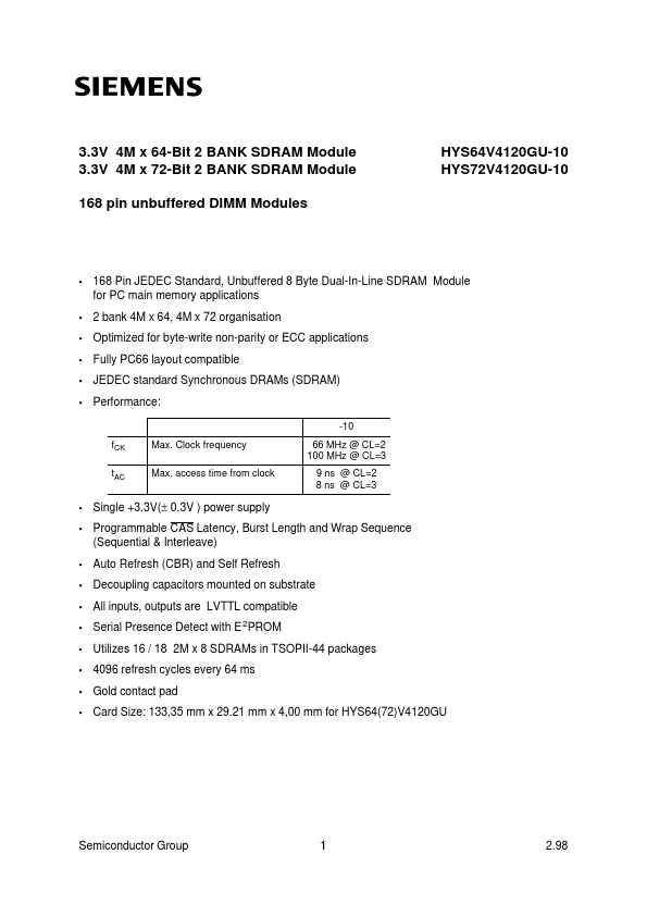
3.3V 4M x 64-Bit 2 BANK SDRAM Module 3.3V 4M x 72-Bit 2 BANK SDRAM Module 168 pin unbuffered DIMM Modules HYS64V4120GU-10 HYS72V4120GU-10 • 168 Pin JEDEC Standard, Unbuffered 8 Byte Dual-In-Line SDRAM Module for PC main memory applications 2 bank 4M x 64, 4M x 72 organisation Optimized for byte-write non-parity or ECC applications Fully PC66 layout compatible JEDEC standard Synchronous DRAMs (SDRAM) Performance: -10 fCK tAC Max. Clock frequency Max. access time from clock 66 MHz @ CL=2 100 MHz @ CL=3 9 ns @ CL=2 8 ns @ CL=3 • • • • • • • Single +3.3V(± 0.
Published: |