Description
Advanced trench technology to provide
excellent RDS(ON), low gate charge and low operation voltage.This device is suitable for using as a load switch or in PWM applications.
Simple Drive Requirement
Small Package Outline
Surface Mount Device
Features
- For a single MOSFET.
- VDS = 70V.
- RDS(ON) = 6.3mΩ @ VGS=10V
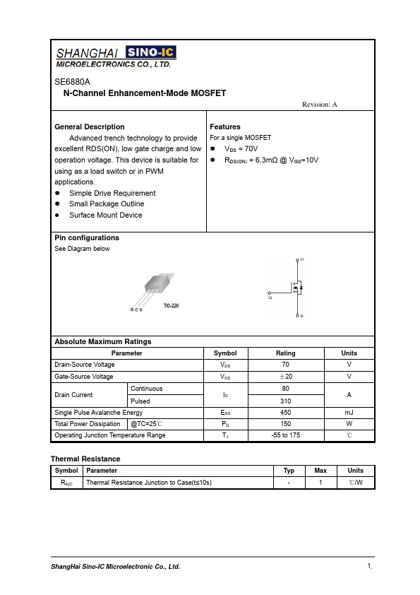
Pin configurations
See Diagram below
Absolute Maximum Ratings
Parameter
Drain-Source Voltage
Gate-Source Voltage
Drain Current
Continuous Pulsed
Single Pulse Avalanche Energy
Total Power Dissipation @TC=25℃
Operating Junction Temperature Range
Symbol VDS VGS
ID
EAS PD TJ
Thermal Resistance
Symbol Parameter RθJC Thermal Resistance Junction to Case(t≤10s)
Rating 70 ±20 80 310 450 150
-55 to 175
Units V V
A
mJ W ℃
Ty.
 SE6880A-Sino-IC.pdf