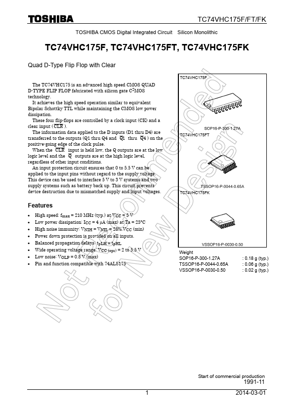
TC74VHC175FK
Overview
- High speed: fmax = 210 MHz (typ.) at VCC = 5 V
- Low power dissipation: ICC = 4 μA (max) at Ta = 25°C
- High noise immunity: VNIH = VNIL = 28% VCC (min)
- Power down protection is provided on all inputs.
- Balanced propagation delays: tpLH ∼- tpHL
- Wide operating voltage range: VCC (opr) = 2 to 5.5 V
- Low noise: VOLP = 0.8 V (max)
- Pin and function compatible with 74ALS175