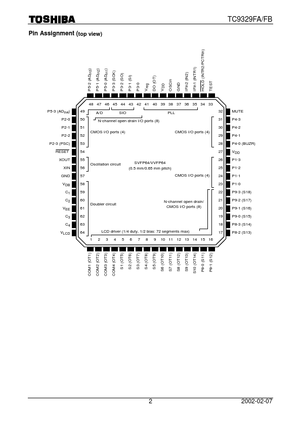
Description
of Pin Function
TC9329FA/FB
Pin No.Symbol
Pin Name
Function and Operation
1 COM1/OT1 2 COM2/OT2 3 COM3/OT3 4 COM4/OT4
S1/OT5~ 5~14
S10/OT14
P8-0/S13~ 15~22
P9-3/S18
Output common signals to LCD panels.Through a matrix with pins S1 to S22, a maximum 88 segments can be displayed.LCD common output/Output port
Three levels, VLCD, VEE, and GND, are output at 62.5 Hz every 2 ms.VEE is output after system reset and CLOCK STOP are released, and a common signal is output after the DISP OFF bi
Features
- built-in 1/4 duty, 1/2 bias and a 3 V voltage doubler boosting circuit, implementing stable LCD. The power supply voltage ranges from 0.9 to 1.8 V. Because of its low-current consumption (CPU: 80 µA (max)), the device is suitable for use in digital tuning systems in portable equipment such as headphone stereos. TC9329FA
Features
TC9329FB.
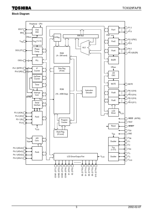
- CMOS DTS microcontroller LSI with built-in 230 MHz prescaler, PLL, and LCD driver.
- Operating voltage: VDD = 0.9~1.8 V (typ. : 1.5 V).
 TC9329FA-Toshiba.pdf