Datasheet Details
| Part number | CHX2091 |
|---|---|
| Manufacturer | United Monolithic Semiconductors |
| File Size | 84.78 KB |
| Description | 20-40GHz Frequency Multiplier |
| Datasheet |
 CHX2091 Datasheet CHX2091 Datasheet
|
|
|
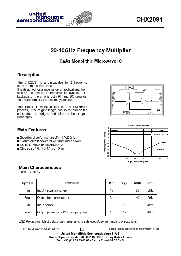
The CHX2091 is a cascadable by 2 frequency multiplier monolithic circuit.
It is designed for a wide range of applications, from military to commercial communication systems.
The backside of the chip is both RF and DC grounds.
| Part number | CHX2091 |
|---|---|
| Manufacturer | United Monolithic Semiconductors |
| File Size | 84.78 KB |
| Description | 20-40GHz Frequency Multiplier |
| Datasheet |
CHX2091 Datasheet
|
|
|
|