Datasheet4U Logo Datasheet4U.com

NJ8820 Datasheet - Zarlink Inc

NJ8820_ZarlinkSemiconductorInc.pdf

Preview of NJ8820 PDF
NJ8820 Datasheet Preview Page 2 NJ8820 Datasheet Preview Page 3

Datasheet Details

Part number:

NJ8820

Manufacturer:

Zarlink Inc

File Size:

493.92 KB

Description:

Frequency synthesiser (prom interface).

NJ8820, FREQUENCY SYNTHESISER (PROM INTERFACE)

Pin no.

1 Name PDA Description Analog output from the sample and hold phase comparator for use as a ‘fine’ error signal.

Output at (VDD2VSS)/2 when the system is in lock.

Voltage increases as fv phase lead increases; voltage decreases as fr phase lead increases.

Output is linear over only a narrow

Obsolescence Notice This product is obsolete.

This information is available for your convenience only.

For more information on Zarlink’s obsolete products and replacement product lists, please visit http://products.zarlink.com/obsolete_products/ THIS DOCUMENT IS FOR MAINTENANCE PURPOSES ONLY AND IS NOT RECOMMENDED FOR NEW DESIGNS NJ8820 DS3277-1.2 NJ8820 FREQUENCY SYNTHESISER (PROM INTERFACE) The NJ8820 is a synthesiser circuit fabricated on the GPS CMOS process and is capable of achieving h

NJ8820 Features

* s s s s Low Power Consumption Direct Interface to ROM or PROM High Performance Sample and Hold Phase Detector >10MHz Input Frequency 
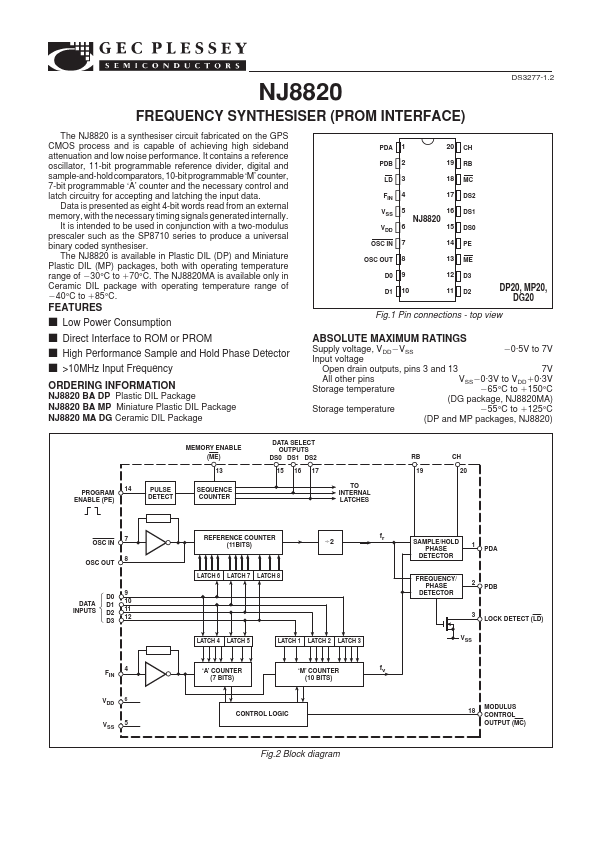
Fig.1 Pin connections - top view ABSOLUTE MAXIMUM RATINGS 20

* 5V to 7V Supply voltage, VDD2VSS Input voltage 7V Open drain outputs, pins 3 and 13 VSS20

* 3V t

📁 Related Datasheet

📌 All Tags

Zarlink Inc NJ8820-like datasheet