Click to expand full text
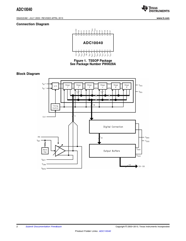
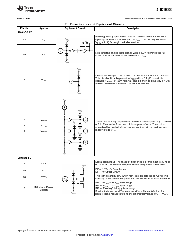
ADC10040
www.ti.com
SNAS224M – JULY 2003 – REVISED APRIL 2013
ADC10040/ADC10040Q 10-Bit, 40 MSPS, 3V, 55.5 mW A/D Converter
Check for Samples: ADC10040
FEATURES
1
•2 Single +3.0V Operation • Selectable 2.0 VP-P, 1.5 VP-P, or 1.0 VP-P full-
scale input swing • 400 MHz −3 dB Input Bandwidth • Low Power Consumption • Standby Mode • On-Chip Reference and Sample-and-Hold
Amplifier • Offset Binary or Two’s Complement Data
Format • Separate Adjustable Output Driver Supply to
Accommodate 2.5V and 3.3V Logic Families • AEC-Q100 Grade 3 Qualified • 28-Pin TSSOP Package
KEY SPECIFICATIONS
• Resolution: 10 Bits • Conversion Rate: 40 MSPS • Full Power Bandwidth: 400 MHz • DNL: ±0.3 LSB typ) • SNR (fIN = 11 MHz): 59.6 dB (typ) • SFDR (fIN = 11 MHz): -80 dB (typ) • Power Consumption, 40 MHz: 55.
 ADC10040 Datasheet