CDCLVD2102
FEATURES
- Dual 1:2 Differential Buffer
- Low Additive Jitter <300 fs RMS in 10-k Hz to
20-MHz
- Low Within Bank Output Skew of 15 ps (Max)
- Universal Inputs Accept LVDS, LVPECL,
LVCMOS
- One Input Dedicated for Two Outputs
- Total of 4 LVDS Outputs, ANSI EIA/TIA-644A
Standard patible
- Clock Frequency up to 800 MHz
- 2.375- 2.625V Device Power Supply
- LVDS Reference Voltage, VAC_REF, Available for
Capacitive Coupled Inputs
- Industrial Temperature Range
- 40°C to 85°C
- Packaged in 3mm × 3mm 16-Pin QFN (RGT)
- ESD Protection Exceeds 3 k V HBM, 1 k V CDM
APPLICATIONS
- Telemunications/Networking
- Medical Imaging
- Test and Measurement Equipment
- Wireless munications
- General Purpose Clocking
DESCRIPTION
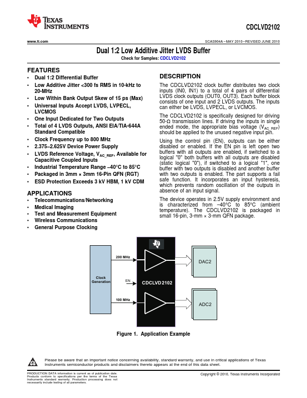
The CDCLVD2102 clock buffer distributes two clock inputs (IN0, IN1) to a total of 4 pairs of differential LVDS clock outputs (OUT0, OUT3). Each buffer block consists of one input and 2 LVDS outputs. The inputs can either be LVDS, LVPECL, or LVCMOS.
The CDCLVD2102 is specifically...