Datasheet Details
| Part number | SN74AUC126 |
|---|---|
| Manufacturer | Texas Instruments ↗ |
| File Size | 816.78 KB |
| Description | QUADRUPLE BUS BUFFER GATE |
| Datasheet |
 SN74AUC126-etcTI.pdf SN74AUC126-etcTI.pdf
|
| Part number | SN74AUC126 |
|---|---|
| Manufacturer | Texas Instruments ↗ |
| File Size | 816.78 KB |
| Description | QUADRUPLE BUS BUFFER GATE |
| Datasheet |
SN74AUC126-etcTI.pdf
|
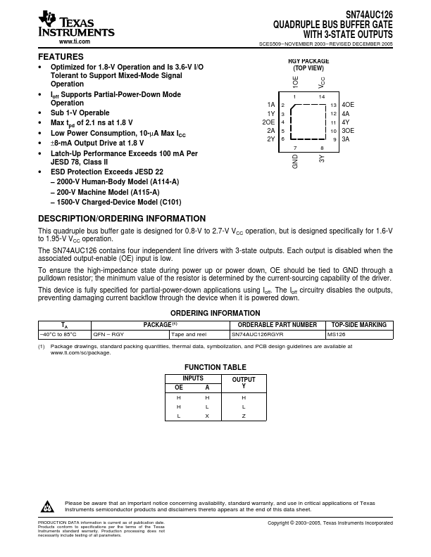
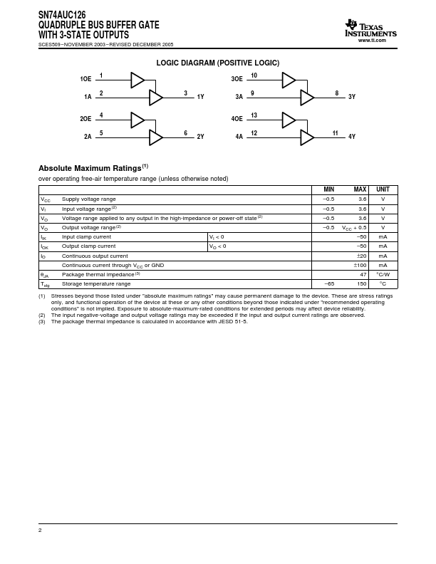
ORDERING INFORMATION This quadruple bus buffer gate is designed for 0.8-V to 2.7-V VCC operation, but is designed specifically for 1.6-V to 1.95-V VCC operation.The SN74AUC126 contains four independent line drivers with 3-state outputs.Each output is disabled when the associated output-enable (OE) input is low.To ensure the high-impedance state during power up or power down, OE should be tied to GND through a pulldown resistor; the minimum value of the resistor is determined by the current-so
📁 SN74AUC126 Similar Datasheet