Datasheet Details
| Part number | SN74LV367A |
|---|---|
| Manufacturer | Texas Instruments ↗ |
| File Size | 1.00 MB |
| Description | HEX BUFFERS AND LINE DRIVER |
| Datasheet |
 SN74LV367A-etcTI.pdf SN74LV367A-etcTI.pdf
|
| Part number | SN74LV367A |
|---|---|
| Manufacturer | Texas Instruments ↗ |
| File Size | 1.00 MB |
| Description | HEX BUFFERS AND LINE DRIVER |
| Datasheet |
SN74LV367A-etcTI.pdf
|
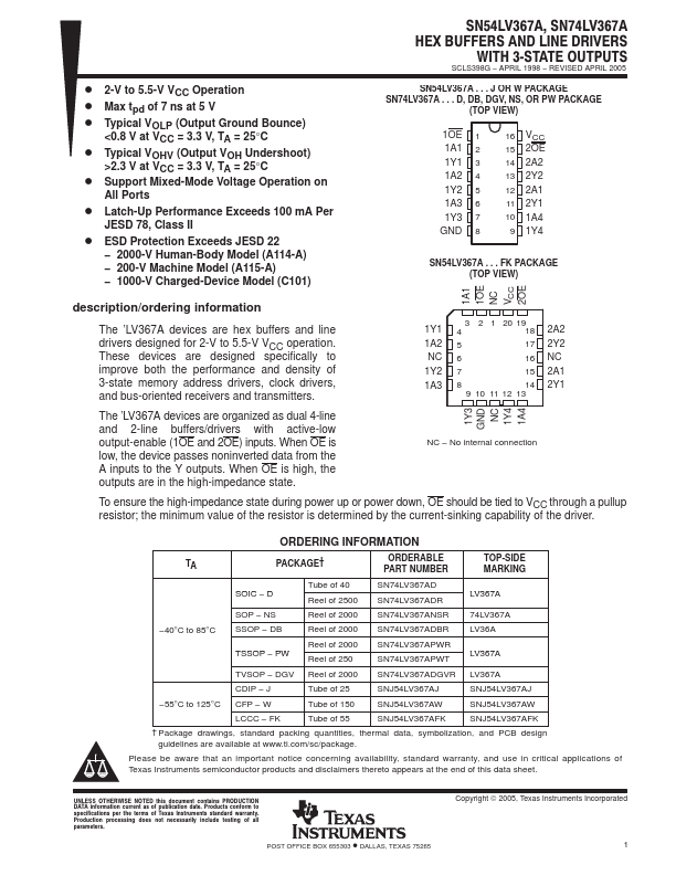
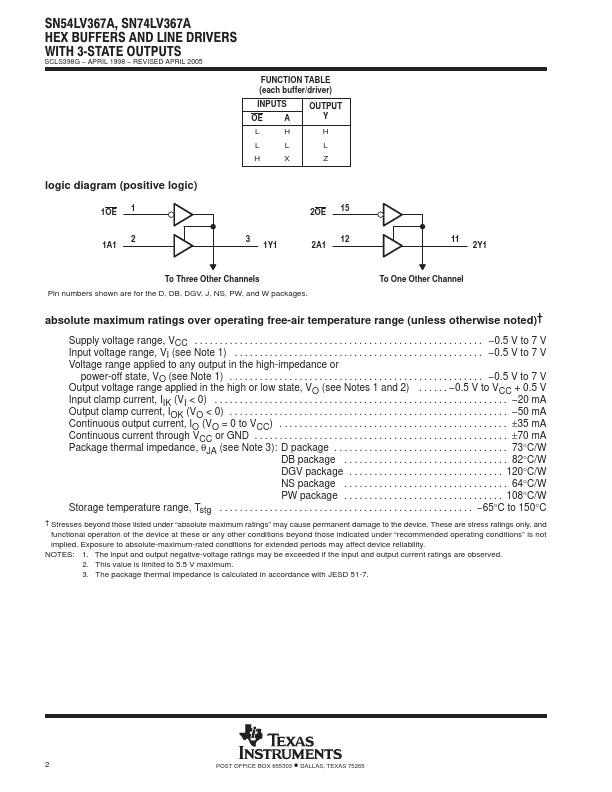
ordering information The ’LV367A devices are hex buffers and line drivers designed for 2-V to 5.5-V VCC operation.These devices are designed specifically to improve both the performance and density of 3-state memory address drivers, clock drivers, and bus-oriented receivers and transmitters.1Y1 3 2 1 20 19 4 18 2A2 1A2 5 17 2Y2 NC 6 16 NC 1Y2 7 15 2A1 1A3 8 14 2Y1 9 10 11 12 13 1Y3 GND NC 1Y4 1A4 The ’LV367A devices are organized as dual 4-line and 2-line buffers/drivers with a
📁 SN74LV367A Similar Datasheet