Datasheet Details
| Part number | SN74LVC2952A |
|---|---|
| Manufacturer | Texas Instruments ↗ |
| File Size | 385.99 KB |
| Description | OCTAL BUS TRANSCEIVER AND REGISTER |
| Datasheet |
 SN74LVC2952A-etcTI.pdf SN74LVC2952A-etcTI.pdf
|
| Part number | SN74LVC2952A |
|---|---|
| Manufacturer | Texas Instruments ↗ |
| File Size | 385.99 KB |
| Description | OCTAL BUS TRANSCEIVER AND REGISTER |
| Datasheet |
SN74LVC2952A-etcTI.pdf
|
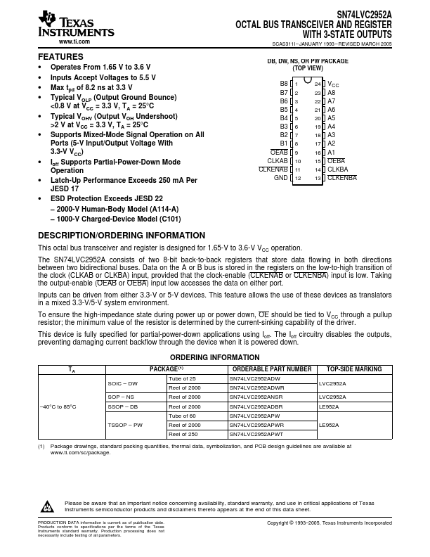
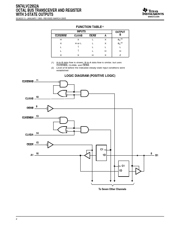
ORDERING INFORMATION This octal bus transceiver and register is designed for 1.65-V to 3.6-V VCC operation.The SN74LVC2952A consists of two 8-bit back-to-back registers that store data flowing in both directions between two bidirectional buses.Data on the A or B bus is stored in the registers on the low-to-high transition of the clock (CLKAB or CLKBA) input, provided that the clock-enable (CLKENAB or CLKENBA) input is low.Taking the output-enable (OEAB or OEBA) input low accesses the data on
📁 SN74LVC2952A Similar Datasheet