Datasheet4U Logo Datasheet4U.com

SN74LVC2G125-Q1 Dual Bus Buffer Gate

SN74LVC2G125-Q1 Description

SN74LVC2G125-Q1 www.ti.com DUAL BUS BUFFER GATE WITH 3-STATE OUTPUTS Check for Samples: SN74LVC2G125-Q1 SCES559C * MARCH 2004 * REV.
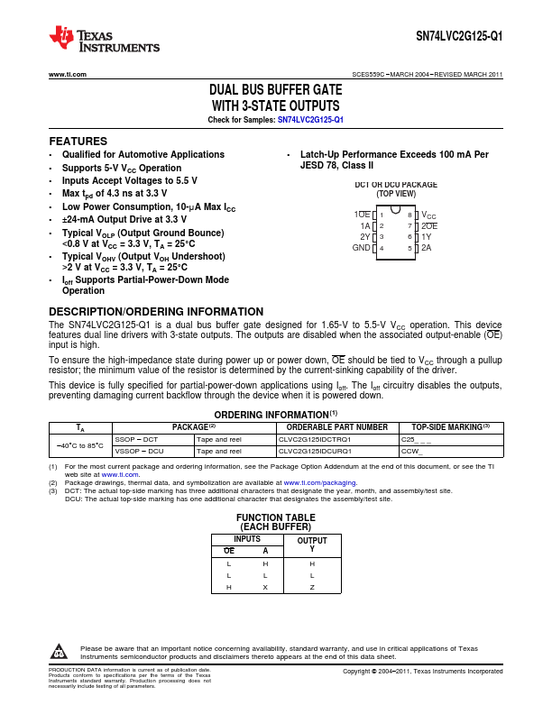
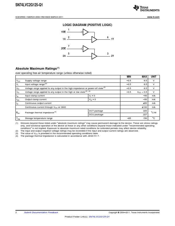
ORDERING INFORMATION The SN74LVC2G125-Q1 is a dual bus buffer gate designed for 1.

SN74LVC2G125-Q1 Features

* 1

SN74LVC2G125-Q1 Applications

* Supports 5-V VCC Operation
* Inputs Accept Voltages to 5.5 V
* Max tpd of 4.3 ns at 3.3 V
* Low Power Consumption, 10-μA Max ICC
* ±24-mA Output Drive at 3.3 V
* Typical VOLP (Output Ground Bounce)

📥 Download Datasheet

Preview of SN74LVC2G125-Q1 PDF
datasheet Preview Page 2 datasheet Preview Page 3

📁 Related Datasheet

  • SN74LVC1G125 - high performance non-inverting buffer (UMW)
  • SN74LVC1G34 - Single buffer (UMW)
  • SN74L71 - AND-Gate R-S Master-Slave F-F (National Semiconductor)
  • SN74L74N - Dual D-Type Flip-Flop (ETC)
  • SN74LS00 - QUAD 2-INPUT NAND GATE (Motorola)
  • SN74LS02 - QUAD 2-INPUT NOR GATE (Motorola)
  • SN74LS04 - Hex Inverter (ON Semiconductor)
  • SN74LS04D - Hex Inverter (ON Semiconductor)

📌 All Tags

Texas Instruments SN74LVC2G125-Q1-like datasheet