Datasheet4U Logo Datasheet4U.com

SN74LVC2G80 Dual Positive-Edge-Triggered D-Type Flip-Flop

SN74LVC2G80 Description

SN74LVC2G80 www.ti.com SCES309F * DECEMBER 2001 * REVISED DECEMBER 2013 Dual Positive-Edge-Triggered D-Type Flip-Flop Check for Samp.
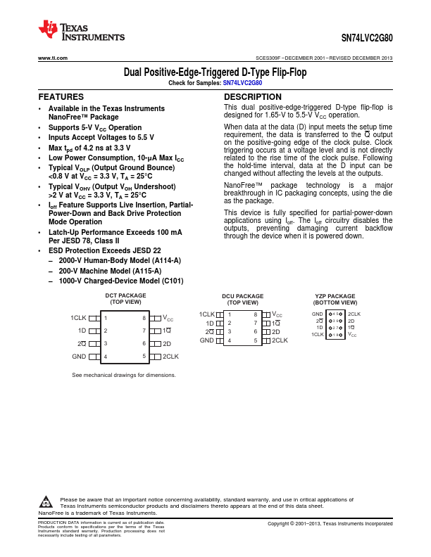
This dual positive-edge-triggered D-type flip-flop is designed for 1.

SN74LVC2G80 Features

* 1
* 2 Available in the Texas Instruments NanoFree™ Package
* Supports 5-V VCC Operation
* Inputs Accept Voltages to 5.5 V
* Max tpd of 4.2 ns at 3.3 V
* Low Power Consumption, 10-μA Max ICC
* Typical VOLP (Output Ground Bounce)

SN74LVC2G80 Applications

* using Ioff. The Ioff circuitry disables the outputs, preventing damaging current backflow through the device when it is powered down. 1CLK 1D 2Q GND DCT PACKAGE (TOP VIEW) 18 27 36 45 VCC 1Q 2D 2CLK 1CLK 1D 2Q GND DCU PACKAGE (TOP VIEW) 18 27 36 45 VCC 1Q 2D 2CLK YZP PACKAGE (BOTTOM VIEW) GND

📥 Download Datasheet

Preview of SN74LVC2G80 PDF
datasheet Preview Page 2 datasheet Preview Page 3

📁 Related Datasheet

  • SN74LVC1G125 - high performance non-inverting buffer (UMW)
  • SN74LVC1G34 - Single buffer (UMW)
  • SN74L71 - AND-Gate R-S Master-Slave F-F (National Semiconductor)
  • SN74L74N - Dual D-Type Flip-Flop (ETC)
  • SN74LS00 - QUAD 2-INPUT NAND GATE (Motorola)
  • SN74LS02 - QUAD 2-INPUT NOR GATE (Motorola)
  • SN74LS04 - Hex Inverter (ON Semiconductor)
  • SN74LS04D - Hex Inverter (ON Semiconductor)

📌 All Tags

Texas Instruments SN74LVC2G80-like datasheet